Microstructure and Integrity of Thin Silicon Films on Sio 2 after Immersion in 10:1 Buffered HF
- PDF / 2,255,653 Bytes
- 6 Pages / 414.72 x 648 pts Page_size
- 11 Downloads / 226 Views
MICROSTRUCTURE AND INTEGRITY OF THIN SILICON FILMS ON Si02 AFTER IMMERSION IN 10:1 BUFFERED HF
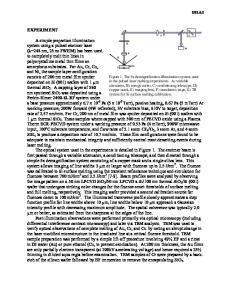
RAMA I. HEGDE, MARK A. CHONKO AND PHILIP J. TOBIN Advanced Products Research and Development Laboratory Motorola, Inc., Austin, Texas 78721
ABSTRACT The microstructure and integrity of thin silicon films on Si02 after immersion in 10:1 buffered HF solution were investigated by AES, AFM and TEM measurements. Silicon films of 30 nm - 50 nm thicknesses were deposited on 15 nm of thermal oxide by LPCVD using SiH4 at 550 oC, 580 oC and 625 oC. These films were then treated with the HF for 15 seconds and characterized systematically. The data provided direct physical evidence for etching of gate oxide by the HF solution through defects (holes) in the 580 °C Si film. INTRODUCTION Earlier, we reported on growth and surface morphology of thin silicon films deposited over a range of temperature (550 oC to 625 OC) using an AFM [1]. A close relationship was established between the electrical breakdown of capacitors fabricated using the HF exposed thin silicon films as the bottom layer of a split gate capacitor and the roughness of the bottom layer [2]. The cumulative breakdown distribution was found to shift to higher voltages with a decrease of surface roughness. Here we report on recent AFM, TEM and AES data that provided a direct physical evidence for etching of underlying gate oxide by HF solution through defects in the Si film. EXPERIMENTS Silicon films of 30 nm - 50 nm thicknesses were deposited on 15 nm of thermal oxide (Si0 2 ) by conventional LPCVD using SiH4 at 550 °C, 580 oC and 625 oC [1 - 3]. These thin thin Si films were investigated by AFM, AES and TEM measurements. The continuity of the 2 6 Si films was evaluated electrically by fabricating MOS capacitors with an area of 3x10 .m , using a split gate electrode deposition process. Approximately 30 nm of LPCVD silicon film was deposited on 15 nm of thermal oxide at the temperatures given above. These Si films were then etched for 15 seconds in 10:1 H20 : HF prior to a second 275 nm Si film deposition at 625 OC. Any voids or discontinuities in the first Si layer will allow the HF solution to reach the gate oxide resulting in a degraded breakdown voltage. In a separate experiment, the thin Si films of each type were immersed in 10:1 buffered HF at room temperature to check the integrity of the underlying gate oxide layer. Thus AFM, AES and TEM measurements were obtained for the thin Si films with and without buffered HF treatment. RESULTS AND DISCUSSION Fig. I shows the cumulative breakdown distributions of the capacitors fabricated using thin silicon films deposited at three temperatures, as the bottom layer of a split gate capacitor. Complete shorting was observed for the capacitor fabricated with the 580 °C Si film. This
Mat. Res. Soc. Symp. Proc. Vol. 297. Ic)1993 Materials Research Society
1038
suggests complete lack of protection of the gate oxide for the 580 oC Si film. Some improvement in the breakdown distribution occurs for the 625 oC film, but only the 550
Data Loading...