Microstructure and Strain in GaAs/AlGaAs MQW thin Films Bonded to Different Substrates by Eutectic Alloying
- PDF / 1,360,444 Bytes
- 6 Pages / 414.72 x 648 pts Page_size
- 48 Downloads / 307 Views
INTRODUCTION Eutectic metal bonding (EMB) has been widely used in flip chip bonding, also, it has attracted intensive studies for further applications in optoelectronic integrated circuits (OEIC)[1][2]. Au-Sn, Pb-Sn, Au-Ge and Au-Si are the eutectic systems commonly used in optoelectronic integration[3][4][5]. Among these solders, Au-Sn eutectic alloy possesses the features of high strength, suitable eutectic point and good reliability. Au-Sn alloy exhibits elastic deformation during thermal cycling due to high strength. It also provides a good ohmic contact for GaAs/AlGaAs system. Recently, we have reported the creation of in-plane anisotropic strain in GaAs/ AIGaAs MQW thin film bonded on LiTaO 3 by using optical glue and Au-Sn eutectic alloy[6][7]. The bonded MQWs exhibited an optical anisotropy resulting from an in-plane anisotropic strain[81. A new class of optoelectronic device taking advantages of the thermally induced anisotropic strain can be developed. In this report, we extend our previous work of the Au-Sn eutectic bonding and present the study of microstructure in the bonding interface and analysis of thermally induced strain in the MQWs bonded to different materials. 331
Mat. Res. Soc. Symp. Proc. Vol. 356 0 1995 Materials Research Society
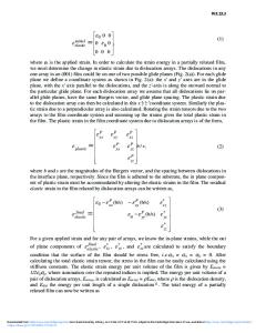
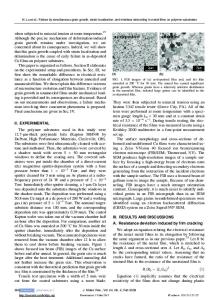
EXPERIMENTAL Samples used in this study include MQW thin films bonded to GaAs, Si and Y-cut LiNbO 3 submount substrates. The p-i(MQW)-n structures were grown in a Varian Gen HI MBE on (100) GaAs semi-insulating substrates. The layer sequence of the p-i(MQW)-n structures includes a 500A AlAs layer serving as an etching-stop, a 3000A n+-type (10 'cm3) Al 0.3Ga0, 7As and a 500A Al . Ga .7As spacer followed by the MQW structure consisting 03 0 of 150 periods of 80A GaAs/60A A10. 3Ga 0 .7As, then 500A A10.3Ga0 .7As spacer and 4000A p+-type (10 18 cm-3) Alo. 3Ga 0.7As layer. The whole wafers were then subjected to backside processing. The samples were lapped down to 150 jim, then polished with a bromine methanol (3 wt% Br + CH 3 OH) solution to IOOjim. The bonding layer used here is the eutectic
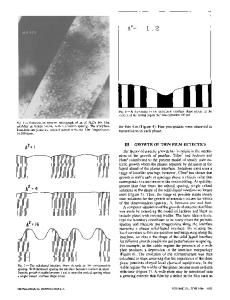
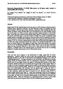
alloy with the composition of 80 wt% Au and 20 wt% Sn ( totally 0.95 jim). The Cr (500 A) layer was first deposited as an adhesion and barrier layer onto the MQW samples and submount substrates followed by eutectic layer deposition. The thin films and submounts were then brought into intimate contact under static pressure, then put in a furnace. The samples were annealed at 370TC under forming gas (1000ppm H2 + N 2) ambient for 15 minutes, then cooled down to room temperature in different routes as depicted in figure 1. After bonding, the lift-off or backside etching process was carried out to remove the remained GaAs substrates on the bonded pi(MQW)-n samples. The citric acid solution was used to etch the GaAs substrates with the etching selectivity of GaAs to AlAs over 500:1, and GaAs etching rate is about 3000A/min[9]. The residual AlAs was then removed by buffered HF solution.
400-
~300
0i)
200.
0 0
Annealing Time (min) Processing (i): Samples cooled in a furnace til
Data Loading...