Structural characterization of 3C-SiC films grown on Si layers wafer bonded to polycrystalline SiC substrates
- PDF / 991,296 Bytes
- 4 Pages / 595 x 842 pts (A4) Page_size
- 102 Downloads / 375 Views
J5.23.1
Structural characterization of 3C-SiC films grown on Si layers wafer bonded to polycrystalline SiC substrates R.L. Myers,1) K.D. Hobart,2) M. Twigg,2) S. Rao,1) M. Fatemi,2) Saddow,*1)
F.J. Kub,2) and S.E.
1)
Electrical Engineering Department, University of South Florida, Tampa, FL 33620 Naval Research Laboratory, Code 6813, Washington, DC 20375 * TEL: +813.974.4773, FAX: +813.974.5250, EMAIL: [email protected]
2)
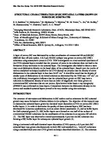
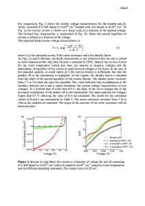
Abstract Single crystal 3C-SiC epitaxial layers have been grown on SOI substrates using low-pressure chemical vapour deposition (LPCVD). The SOI substrates consist of nominally 150 Å Si layers bonded to 100 mm poly 3C-SiC substrates using direct wafer bonding and SOI film transfer techniques. Miscut Si(100) films were incorporated into the wafer bonding process for the first time in an effort to further reduce anti-phase domain formation in the 3C-SiC films. The Si films were transferred from Si(100) wafers miscut 4° toward the (110) direction. For growth of 3C-SiC layers, a two-step process is needed. First the Si is carbonized using propane mixed in a hydrogen carrier gas to convert the surface to SiC at atmospheric pressure. Next SiC growth is conducted by the addition of silane into the gas mix and a reduction of the process to 150 Torr. Previous characterization of these films via SEM and XRD indicated that the films were single crystal and oriented with respect to the starting Si bonded film. In this work we present results of TEM analysis of these films which show details of the atomic structure at the 3C-SiC/poly-crystalline SiC interface where a thin (6 nm thick) amorphous region has been detected, likely due to SiO2 used to wafer bond the Si film to the poly substrate. A detailed study of this material system is presented with the aim of providing feedback for possible improvements in the 3C-SiC growth process. Introduction There has been much progress in the development of single crystal SiC for device applications. However, defects are still an issue with commercial SiC substrates having micropipe densities on the order of 50 pipes/cm2 and dislocation densities on the order of 10,000 dislocations/cm2. The large anisotropy in 4H- and 6H-SiC, the difficulties in heavily doping 4H-SiC for bipolar devices, and the unsatisfactory performance of 4H-SiC MOS devices have all encouraged interest once again in producing device-quality 3C-SiC films. The lattice mismatch between the Si substrate and the grown SiC produces planar defects in the film. In the past two decades, progress has been made on reducing these effects, however, the films are not yet of device quality. Hobart et. al. reported on the transfer of ultra-thin Si layers onto polycrystalline SiC substrates with the specific goal of using this ‘SOI’ or composite substrate for high-temperature growth of 3C-SiC [1]. We recently reported growth on these substrates, which were miscut 4º toward the [211] direction, using LPCVD to produce single crystal 3C-SiC films [2]. While these preliminary results are encouraging, a more in-depth ch
Data Loading...