Mixing in PCBM/P3HT bilayers, using in situ and ex situ neutron reflectivity
- PDF / 684,127 Bytes
- 11 Pages / 584.957 x 782.986 pts Page_size
- 12 Downloads / 394 Views
hilipp Gutfreund Large Scale Structures, Institut Laue-Langevin, Grenoble 38000, France
David James College of Engineering, Swansea University, Wales SA1 8EN, UK (Received 2 August 2016; accepted 30 January 2017)
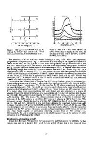
In situ and ex situ neutron reflectivity is used to characterize annealed regioregular-P3HT/PCBM bilayers. In situ annealing of a 20 nm PCBM/35 nm P3HT bilayer at 170 °C reveals rapid mixing of PCBM and P3HT to produce a polymer-rich layer that contains around 18–20% PCBM. Samples with three different thicknesses of P3HT layer are ex situ annealed at 140 °C. This again reveals migration of PCBM into the P3HT and vice versa, with the polymer-rich layer in the 20 nm PCBM/ 35 nm P3HT sample containing 19% PCBM. Complete migration of the entire PCBM layer into the P3HT layer is observed for a 20 nm PCBM/80 nm P3HT bilayer. The robustness of fitted model composition profiles, in comparison with real-space imaging of sample surface morphology and previous work on annealed P3HT/PCBM bilayer compositions, is discussed in detail.
I. INTRODUCTION
Organic photovoltaic (OPV) devices offer the potential for low-cost and large-area solar cells.1 Ultrathin and flexible OPV devices also enable building and transport integration in products such as windows, transparent roofs, or car windshields.2,3 OPVs are particularly attractive because of the ability to manufacture them using high throughput printing processes.4 A popular choice for the active layer of OPVs is the bulk heterojunction (BHJ) formed by blending together electron-donating and electron-accepting species (either polymers or small molecules). A long-established and well-studied choice for such a blend consists of a fullerene derivative and a conjugated polymer.5,6 Here, the BHJ consists of a complex morphology that is designed to enable efficient separation of charges at the interface between the electrondonating polymer and the electron-accepting fullerene.7 The requirement for large interfacial area needs to be balanced by the provision of a continuous path for electron and hole transport.7 A full characterization and understanding of the morphology formed during device fabrication, and the potential evolution of structure/morphology during operation,8 is challenging because a number of different processes, such as phase separation, surface or Contributing Editor: Dean DeLongchamp a) Address all correspondence to this author. e-mail: [email protected] DOI: 10.1557/jmr.2017.59
substrate enrichment9 and crystallization (potentially of both components),2,6 may contribute to the final film structure and device performance. It is hoped that the development of further understanding of the morphology of OPV materials in thin-film architectures will underpin the successful commercial application of OPVs.2,5,10,11 This paper describes a study that focusses on conjugated polymer/fullerene mixing, by looking at the evolution of morphology within a simplified (bilayer) geometry, as a function of the polymer film thickness and temperature. To understand the process cont
Data Loading...