Mo and Co Silicide FEAs
- PDF / 9,222,118 Bytes
- 9 Pages / 612 x 792 pts (letter) Page_size
- 22 Downloads / 349 Views
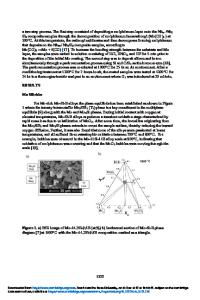
Mo and Co Silicide FEAs Jong Duk Lee, Byung Chang Shim, Sung Hun Jin and Byung-Gook Park Inter-University Semiconductor Research Center(ISRC) and School of Electrical Engineering, Seoul National University, San 56-1, Shinlim-dong, Kwanak-gu, Seoul 151-742, Korea ABSTRACT For enhancement and stabilization of electron emission, Mo and Co silicides were formed from Mo mono-layer and Ti/Co bi-layers on single crystal silicon FEAs, respectively. Using the slope of Fowler-Nordheim curve and tip radius measured from SEM, the effective work function of Mo and Co silicide FEAs are calculated to be 3.13 eV and 2.56 eV, respectively. Compared with silicon field emitters, Mo and Co silicide exhibited 10 and 34 times higher maximum emission current, 10 V and 46 V higher failure voltage, and 6.1 and 4.8 times lower current fluctuation, respectively. Moreover, the emission currents of the silicide FEAs depending on vacuum level are almost same in the range of 10-9 ∼ 10-6 torr. This result shows that silicide is robust in terms of anode current degradation due to the absorption of air molecules. INTRODUCTION Metal silicides including Ti [1, 2], Co [2, 3], Nb [4], Mo [5, 6], Pd [7, 8], Cr [9] and Pt [10] were previously reported in various literatures to improve electron emission characteristics of Si FEAs. The advantages of silicide emitters have been mentioned as lower effective work function, higher electrical conductivity, and better chemical and thermal stability than those of silicon emitters. However, due to different emitter structure design and silicide formation process, the emitter materials including silicide phase and emitter structure including tip radius are not same. Thus, the results presented in the literatures are not always consistent. Therefore, it is still important to study effective work function, and emission current characteristics for the silicide emitters, especially Mo and Co silicides. To obtain the effective work functions, slopes of Fowler-Nordheim (F-N) curves are drawn and tip radii are measured by field emission scanning electron microscopy (FESEM). The emission current fluctuation and stability at a fixed gate bias and the emission current change depending on vacuum pressure will be described. EXPERIMENTAL The 625 tip single crystal silicon(c-Si) FEAs with a gate opening of 1.4 µm were fabricated by dry etching and sharpening oxidation [11]. Some of the c-Si FEAs were splitted for metal deposition and followed by annealing for the silicide emitters. The Mo silicide was formed by coating of 25-nm thick Mo mono-layer on Si-tips and subsequent annealing by rapid thermal process (RTP) at 1000 oC in inert gas (N2) ambient. Coating with Co mono-layer (25 nm), Co/Ti (18 nm/6 nm) and Ti/Co (15 nm/12 nm) bi-layers on Si-tips, and subsequent annealing by RTP at 800 oC, 900 oC and 800 oC in inert gas (N2) ambient produced Co silicides. After formation of R4.1.1
the silicides, the unreacted metals and unwanted by-products were removed by wet etching. As a novel process to form Co silicide by electrical stres
Data Loading...