Modeling and Experiments of Boron Diffusion During Sub-Millisecond Non-Melt Laser Annealing in Silicon
- PDF / 3,360,755 Bytes
- 6 Pages / 612 x 792 pts (letter) Page_size
- 62 Downloads / 391 Views
0912-C05-06
Modeling and Experiments of Boron Diffusion During Sub-Millisecond Non-Melt Laser Annealing in Silicon Taiji Noda1,2, Susan Felch3, Vijay Parihar3, Christa Vrancken4, Tom Janssens4, Hugo Bender4, and Wilfried Vandervorst4 1 Matsushita Electric Industrial Co., Ltd., Kapledreef 75, Leuven, B-3001, Belgium 2 Matsushita assignee at IMEC, Kapledreef 75, Leuven, B-3001, Belgium 3 Appiled Materials, Sunnyvale, CA, 94086 4 IMEC, Kapledreef 75, Leuven, B-3001, Belgium
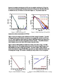
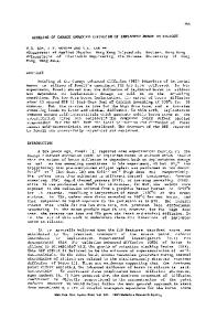
ABSTRACT Boron diffusion and defect evolution during sub-millisecond (ms) laser annealing with partial SPER are investigated using secondary ion mass spectrometry and transmission electron microscopy. Boron diffusivity enhancement in amorphous-Si is observed during partial SPER at 550 ºC. It is shown that boron diffusion during the laser annealing process is a 2-step diffusion (SPER + Laser). The depth of the amorphous layer affects the dopant activation behavior. During sub-ms laser annealing, end-of-range defects are formed and show an evolution behavior. {311} defects cannot completely transfer to dislocation loops after 1300 ºC laser annealing. It is considered that the thermal budget of sub-ms laser is too small for full defect evolution. Atomistic diffusion modeling using a kinetic Monte Carlo method can explain the defect behavior during laser annealing. INTRODUCTION Achievement of diffusion-less annealing is a challenging topic for the sub-45 nm node. For the formation of highly activated and ultra shallow p-type junctions, there are mainly two approaches (1) low temperature Solid phase epitaxial regrowth (SPER) or (2) millisecond or submillisecond annealing [1-5]. Sub-millisecond laser annealing is one of most promising annealing techniques. This annealing can achieve temperatures up to ~ 1350 ºC within 1 ms. Therefore the understanding of dopant diffusion and defect evolution behavior during the sub-millisecond annealing time range is very important. In this work, modeling and experiments of non-melt laser annealing are shown. An atomistic diffusion model using a kinetic Monte Carlo (KMC) method [6,7] for defect evolution during laser annealing is also shown. EXPERIMENT The n-type, 200mm, (100) wafers were implanted with Ge at energies of 5, 8, and 30 keV at a dose of 1×10¹⁵/cm2 for pre-amorphization implant (PAI). Then boron was implanted at an energy of 0.5 keV, 1×10¹⁵/cm2. The depth of the original amorphous/crystalline interface is determined by the Ge PAI condition. Non-melt laser annealing was done at temperatures ranging from 1000 ºC to 1300 ºC.
To improve thermal uniformity during high temperature laser annealing, a low temperature thermal treatment at 550 ºC was performed before laser annealing. SPER is possible at 550 ºC. For the defect study, the influences of laser scan speed and combination annealing (for example, SPER + Laser, spike RTA + Laser) are also investigated. The sheet resistance was measured by a 4-point probe tool. The Boron depth profiles were measured by secondary ion mass spectrometry (SIMS) measurements wit
Data Loading...