Modeling and Experiments of Dopant Diffusion and Defects for Laser annealed Junctions and advanced USJ
- PDF / 1,007,162 Bytes
- 9 Pages / 612 x 792 pts (letter) Page_size
- 60 Downloads / 347 Views
1070-E01-03
Modeling and Experiments of Dopant Diffusion and Defects for Laser annealed Junctions and advanced USJ Taiji Noda1, Wilfried Vandervorst2,3, Susan Felch4, Vijay Parihar4, Christa Vrancken2, and Thomas Y. Hoffmann2 1 Matsushita Electric Industrial Co., Ltd., 19 Nishikujyo-Kasugacho, Minami-ku, Kyoto, 6018413, Japan 2 IMEC, Kapledreef 75, Leuven, B-3001, Belgium 3 K. U. Leuven, Kasteelpark, Arenberg 10, Leuven, B-3001, Belgium 4 Applied Materials, 974 E. Arques Ave. MIS 81280, Sunnyvale, CA, 94085
ABSTRACT Laser annealed junctions and advanced ultra shallow junctions are studied in both atomistic modeling and experiments. SIMS and sheet resistance measurement for spike-RTA + Laser annealing show that additional laser annealing after spike-RTA (“+Laser”) improve the dopant activation level without increasing in junction depth. “+Laser” effect become effective in the combination of low spike-RTA temperature and high laser temperature. This effect is significant for As doped layer. Spike-RTA based junction has a limitation in viewpoint of Rs-Xj trade-off. Laser-only annealing is promising candidate to overcome this limitation. Boron diffusion with laser-only annealing is investigated. An atomistic kinetic Monte Carlo modeling show that BnIm complexes and End-of-Range (EOR) defects are formed during sub-millisecond annealing time range. Impact of F co-implant on Boron diffusion and EOR defect evolution during sub-millisecond annealing are also investigated. INTRODUCTION Achieving diffusion-less annealing is required for the 32 nm technology node and beyond. For the formation of highly activated and ultra-shallow junctions, millisecond (ms) annealing, such as non-melt laser annealing (NLA), is a promising candidate.[1-13] Co-implant can also suppress the transient enhanced diffusion (TED) of dopants and create shallow junctions. The role of co-implanted species is also an interesting topic.[14-20] Millisecond annealing can achieve temperatures up to ~ 1350 ºC within 1 ms. But the dopant diffusion behavior and defect evolution in such very short annealing time range is not known yet. The understanding of dopant diffusion and defect evolution behavior during the submillisecond annealing time range is very important. In this article, our recent studies on modeling and experiments of non-melt laser annealing are shown. An atomistic diffusion model using a kinetic Monte Carlo (KMC) approach [6, 10, 21, 22] is used for the understanding of dopant diffusion and defect evolution.
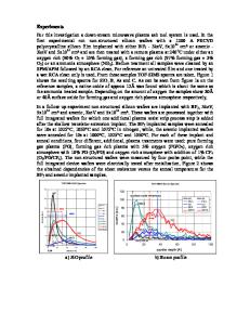
MODELING DESCRIPTION For the accurate modeling of defect evolution and dopant activation during sub-ms annealing with co-implant effects, an atomistic kinetic Monte Carlo (KMC) diffusion model was used. In our KMC model, (1) the depth of the amorphous-Si (a-Si) layer and (2) solid phase epitaxial regrowth (SPER) velocity, which are important for accurate prediction of EOR defect behavior, are modified using experimental results [6, 10]. For the dopant activation/deactivation modeling, dopant-defect complexes, such as BnIm complexes for bor
Data Loading...