Molecular Beam Epitaxial Growth of (Al,Ga)As Tilted Superlattices on Vicinal GaAs (110)
- PDF / 2,688,510 Bytes
- 6 Pages / 420.48 x 639 pts Page_size
- 42 Downloads / 371 Views
MOLECULAR BEAM EPITAXIAL GROWTH OF (AIGa)As TILTED SUPERLATTICES ON VICINAL GaAs (110)
MOHAN KRISHNAMURTHYa, M. WASSERMEIERb, H. WEMANb, J. L. MERZb and P.M. PETROFFa,b, aMaterials Department and bQUEST NSF Science and Technology Center, University of California, Santa Barbara, CA 93106
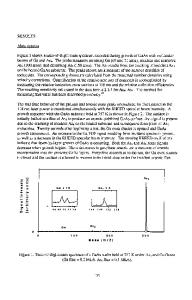
ABSTRACT A study of the molecular beam epitaxial (MBE) growth on singular and vicinal (110) surfaces of GaAs is presented. Quantum well structures and tilted superlattices (TSL) were grown on substrates misoriented 0.5*-2* towards the nearest [010] and [11 ]A azimuths at growth temperatures ranging from 450* C to 600° C under different growth conditions. The structures were characterized by Nomarski optical microscopy, transmission electron microscopy (TEM) and photoluminescence (PL) spectroscopy. Two types of faceting were observed on the surfaces. The structures grown at temperatures above 540"C and As beam fluxes below lxl0-5 torr showed V-shaped facets pointing in the [001] direction and are attributed to As deficient island growth. Lower temperatures and higher As beam fluxes lead to surfaces with microfacets that are elongated along the respective step directions on the vicinal surface and are due to step bunching during growth. Their density and height decrease with decreasing vicinal angle and they disappear on the singular (110) surface. The photoluminescence of the GaAs quantum wells grown on these samples is redshifted with respect to that of the quantum wells grown on the flat surface. This is being ascribed to the fact that on the vicinal surface, the recombination takes place at the facets where the quantum wells are wider. The contrast in the TEM images of the TSL show for the samples misoriented towards [010] that the lateral segregation to the step edges on this surface is appreciable. The TSL spacing and the tilt however show that during growth the vicinal surfaces tend towards a surface with smaller miscut.
INTRODUCTION Growth on vicinal surfaces composed of a periodic step array has become an important technique for the fabrication of nanometer size (9xl0"6 torr until the RHEED shows a sharp but spotty pattern. After the growth of a GaAs buffer layer, the RHEED shows a sharp and streaky pattern with splitting of the specular beam as expected for vicinal surfaces. GaAs and AIGaAs layers were then deposited under various As beam fluxes PAs (measured with an ion gauge at the position of the sample) and substrate temperatures TSub (measured with an infrared pyrometer through a viewport facing the samples). Samples for TEM were prepared by the usual methods of mechanical grinding and ion beam thinning. Dark field images were obtained with a (200) forbidden reflection which is sensitive to the differences in electron scattering between Al and Ga; consequently the bright areas are Al rich and the dark areas are Ga rich [16]. Some of the photo negatives were digitized in an 'Eikonix' digital imaging camera system for subsequent intensity scans. For the PL experiments the 5140 A line from an Ar+ ion laser was used. The
Data Loading...