MOVPE Processes
This chapter discusses the influence of individual QD growth parameters and stacking challenges, along with the material quality and doping levels used for laser device growth. Long wavelength InGaAs QD growth process optimization for applications at \(1.
- PDF / 817,505 Bytes
- 27 Pages / 439.37 x 666.142 pts Page_size
- 31 Downloads / 302 Views
MOVPE Processes
This chapter discusses the influence of individual QD growth parameters and stacking challenges, along with the material quality and doping levels used for laser device growth. For these investigations numerous test samples are grown on a commercially available Aixtron 200/4 MOVPE system. Thus all processes are transferable to industrial mass production systems. The main difference between the employed system and industry production systems is the horizontal flow 3 times 2 inch reactor, versus large multi-wafer reactors for growth on dozens of wafers simultaneously. For economic reasons, all samples of this work are grown with a reactor configuration for either a single 2 inch or a quarter piece of a 2 inch wafer. Further details of the employed MOVPE system are outlined in Sect. 3.1.
4.1 Quantum Dot Growth QD growth optimization for laser applications aims at a maximized optical gain for every individual QD layer. Additionally, stacking optimization is required to generate uniform QD properties across all active layers. In contrast to QW growth, QD epitaxy needs to deal with a non-uniform lateral strain distribution due to the three-dimensional character of the QDs. In particular, the overgrowth of QD layers requires extensive optimization to achieve a perfectly flat surface for all subsequent layers. Details of the basic steps of the employed QD growth process sequence are given in Sect. 3.1.1
4.1.1 QD Optimization Close to 1300 nm InGaAs or I n As QDs in a Ga As matrix with sufficient gain for laser applications are easily tunable within a spectral emission range from 1050 to 1200 nm. To achieve QD
T. D. Germann, Design and Realization of Novel GaAs Based Laser Concepts, Springer Theses, DOI: 10.1007/978-3-642-34079-6_4, © Springer-Verlag Berlin Heidelberg 2012
27
28
4 MOVPE Processes
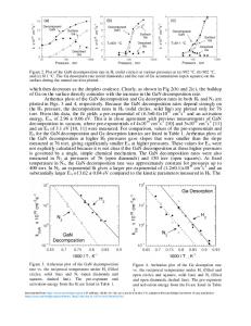
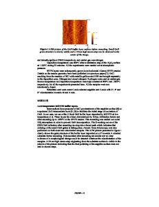
emission close to 1300 nm with high QD areal density, a precise tuning of multiple growth parameters is needed to create a sufficiently large red shift. Achieving QD emission beyond 1300 nm is possible even with I nGa As QDs in a Ga As matrix without any special capping layer, but is linked to a strong reduction in luminescence due to decreased QD density and increased defect formation [1]. The crucial point, however, is to grow long wavelength QD layers closely stacked and with high enough optical quality to generate sufficient gain for laser devices. To assess the optical quality of the QDs and the surrounding matrix material, standardized PL test samples are grown (cf. Sect. 3.3) and characterized using room temperature PL (cf. Sect. 3.2). The Ga As matrix thickness of these PL test structures is already set to the final waveguide thickness of the target laser structure. To investigate the influence of individual parameters usually only a single parameter is changed from run-to-run for the QD optimization process.
QD Growth Temperature Early investigations of the QD formation process showed that higher growth temperatures lead to an increased QD base size, while simultaneously decreasing the QD density
Data Loading...