Narrow Band Gap Amorphous Silicon-Based Solar Cells Prepared by High Temperature Processing
- PDF / 347,460 Bytes
- 6 Pages / 414.72 x 648 pts Page_size
- 59 Downloads / 315 Views
a multi-chamber deposition system; except, for the the argon treatment. The argon treated i-layers were and then the partially completed solar cells were (with exposure to air) for the deposition of the doped 205
Mat. Res. Soc. Symp. Proc. Vol. 507 © 1998 Materials Research Society
layers. The multi-chamber system has demonstrated the ability to prepare 8.4% solar cells (which had neither fully optimized layer thickness nor advanced light trapping enhancements). i-layer thickness were 4000A for all cells repeated here. The doped layers of these solar cells were deposited at various temperatures as summarized in Table 1.
TABLE 1
Doped Layer Deposition Conditions
layer
solar cell structure*
Ts (C)
Si114 flow
CH4 flow
H2 flow
p:a-SiC
PIN
250
3
9
p:j1c-Si n:a-Si
300 200
1 20
33 99 5
p:a-SiC
PIN PIN NIP (RF)
200
3
9
p:a-SiC
NIP (Ar)
250
3
9
p:gtc-Si n:a-Si
NIP NIP (RF)
300 200
1 20
-----
B2H6,PH3 /SiH4 flow 1% 5000ppm 2500ppm
33 33
1%
99 5
5000ppm 2500ppm
1%
5 2500ppm n:a-Si NIP (Ar) 300 20 *Where RF and Ar indicate the i-layer deposited by RF-CVD or by the Argon treatment process (respectively).
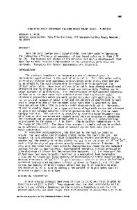
p-i-n solar cells were prepared on a variety of substrates including ZnO coated textured Asahi U type Sn0 2 substrates and smooth Ga-doped ZnO coated glass substrates prepared at a higher temperature process[4]. Typically half of the TCO/glass substrates were over coated with semi transparent evaporated Cr to provide a better diffusion barrier. In the case of n-i-p solar cells the substrates were NiCr coated 7059 (ComingTM Glass) and semitransparent Pt contacts were evaporated onto the p-layers of the completed solar cells. All solar cells were annealed for two hours at 150C after completion of the contact depositions. RESULTS Figure la shows the J-V characteristic of a series of p-i-n solar cells deposited by RFCVD and having a micro-crystalline silicon p-layers as a function of the i-layer deposition temperature. Also, shown is the case of a narrow band gap i-layer prepared by the Ar treatment technique at 300 C. It is clear that the performance markedly decreases with increasing deposition temperature, T,. SIMS (secondary ion mass spectroscopy) analysis of these samples is shown in Fig.2. These results show that sodium ion diffusion at the higher temperatures may be responsible for all or part of the performance loss. The low level B diffusion could not be measured by the SIMS analysis used in this work, because of the textured; therefore, B diffusion from the p-layer could contribute to the performance loss.
206
E Jo - - -------,-250C S..... i -4--220C + 8.o. . . • 1...... 8
"6
......
. ......... ........
:-4-280C -c300C
-
0..... .. --220C c.z.o ..-...
2
C
4' mm .. m-m... 2.....
--4-240C -.- 270C
-.- 300C.......
2 o .o ... ...... -----------2o l
NE
.. ..... .........
Voltage (V)
Voltage (V)
Fig.la
Fig.Ib
jSc-Si Cr/ZnO - ........ ...... .t :. .... ........ .. ....... 2. ...14
** I2 Z 0 i00.1 0.2 0.3 0.40
0
0..
-2200.8.'dr C 25 C * 280.C
20a-SiC
o
4
0
8
Data Loading...