Near-Junction Microfluidic Cooling for Wide Bandgap Devices
- PDF / 666,999 Bytes
- 15 Pages / 432 x 648 pts Page_size
- 82 Downloads / 365 Views
Near-Junction Microfluidic Cooling for Wide Bandgap Devices Avram Bar-Cohen1, Joseph J. Maurer2, and Abirami Sivananthan2 1
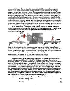
Defense Advanced Research Projects Agency, 675 N. Randolph Street, Arlington, VA 22203. 2 Booz Allen Hamilton, 3811 N. Fairfax Drive, Suite 650, Arlington, VA 22203. ABSTRACT GaN has emerged as the material of choice for advanced power amplifier devices for both industrial and defense applications but near-junction thermal barriers severely limit the inherent capability of high-quality GaN materials. Recent “embedded cooling” efforts, funded by Defense Advanced Research Projects Agency Microsystems Technology Office (DARPA-MTO), have focused on reduction of this near-junction thermal resistance, through the use of diamond substrates and efficient removal of the dissipated power with convective and evaporative microfluidics. An overview of the accomplishments of the DARPA Near-Junction Thermal Transport (NJTT) program and recent results from the on-going DARPA Intra-Chip Embedded Cooling (ICECool) program are provided. It is shown that growth or bonding of diamond to GaN epitaxy has enabled a 3-5× increase in power handling capability per transistor unit area, while use of microfluidic cooling has enabled heat fluxes of 30 kW/cm2 at the transistor level and 1 kW/cm2 at the die-level, for a 3-6× improvement in the total RF output power of GaN power amplifiers. These demonstrations provide near-term validation of the large improvement in output power gained through embedded cooling and confirm the potential for well above a 6× improvement in GaN power amplifier output power to the electrical, rather than thermal, limits of GaN. INTRODUCTION Wide-bandgap materials are poised to revolutionize power electronics, offering higher efficiency, reliability, and output power in a broad range of energy conversion and RF power amplifier (PA) devices. GaN is emerging as the wide bandgap material of choice for both industrial and defense applications and the Defense Advanced Research Projects Agency (DARPA) has made significant progress in extending the state-of-the-art of GaN RF electronics, through programs such as the Wide Band Gap Semiconductors for RF Electronics (WBGS-RF) program [1]. GaN transistors have demonstrated the highest dissipated power density of commercial microwave and millimeter wave semiconductor processes, enabled by their superior fundamental material qualities, including high breakdown voltage and high mobility. As the general evolution of modern electronic systems scales towards increasing levels of integration and packaging density, thermal impediments present a significant bottleneck to realization of the full potential enabled by the GaN material properties. Traditional “remote cooling” solutions, which rely on thermal conduction and spreading through low thermal conductivity substrates and across multiple interfaces, are incapable of limiting device junction temperature rise. Due to the relatively high heat generation rates in GaN transistors, even when grown on relatively higher
Data Loading...