Necessity and relevance of precipitate free clear electrolytes for electrodeposition of CdS semiconductor materials with
- PDF / 2,639,984 Bytes
- 11 Pages / 595.276 x 790.866 pts Page_size
- 11 Downloads / 242 Views
Necessity and relevance of precipitate free clear electrolytes for electrodeposition of CdS semiconductor materials with enhanced photovoltaic properties H. Y. R. Atapattu1 · D. S. M. De Silva1 · K. A. S. Pathiratne1 · O. I. Olusola2 · I. M. Dharmadasa2
Received: 23 June 2017 / Accepted: 28 August 2017 © Springer Science+Business Media, LLC 2017
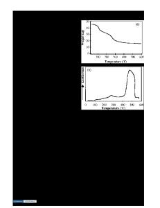
Abstract Cadmium sulfide (CdS) is a well-known window material used for fabrication of second generation thin film solar cells including CdS/CdTe and CdS/CuInGaSe2. Among the CdS fabrication techniques, electrodeposition is a simple, cost effective and scalable method that has been stepped towards large scale commercialization. However, the presence of precipitates in baths used for electrodeposition of CdS has been found to be a persistent problem which had produced CdS thin films with poor photovoltaic properties. Hence, an investigation was carried out to identify a set of optimum physiochemical conditions that can produce clear stable electrolyte for electrodeposition of CdS thin film semiconductors using CdCl2 and Na2S2O3 precursor salts. The study revealed that, electrolytes containing 0.10 mol/L CdCl2 and 0.01 mol/L Na2S2O3, within the pH range of 1.50–2.00 and the temperature range of 55–65 °C can provide clear and stable electrolytes for electrodeposition of CdS thin films. Further, the results showed that, the electrical, optical, morphological and structural properties of CdS layers electrodeposited from electrolytes within above physiochemical conditions were remarkably better to those electrodeposited from the turbid electrolytic baths formed beyond the ranges of predetermined optimum physiochemical conditions.
* D. S. M. De Silva [email protected] 1
Department of Chemistry, University of Kelaniya, Kelaniya, Sri Lanka
2
Materials and Engineering Research Institute, Sheffield Hallam University, Sheffield S1 1WB, UK
1 Introduction Worldwide photovoltaic researches at present are devoted to the development of second generation polycrystalline solar cells including CdS/CdTe and CdS/CuInGaSe2 thin film devices [1, 2]. In these solar cells, CdS semiconductor has a prominent role since the bulk CdS material at room temperature has an energy band gap of 2.42 eV, which transmits most of the photons in the solar spectrum to the CdS/ CdTe and CdS/CuInGaSe2 device junctions. Despite the availability of a wide variety of techniques for fabrication of CdS thin films, electrodeposition (ED) is a preeminent technique owing to its simplicity, low-cost, scalability and manufacturability [3, 4]. In the process of ED, co-deposition of CdS materials formed by processes other than the electrodeposition (e.g. chemical reactions occurring in the bath) and other substances present in the solution are possible and, hence the resulted structural and morphological imperfections attempt to produce poor PV qualities within the CdS layers [3–6]. Therefore, it is essential to take necessary steps to minimize co-deposition of CdS and other substances formed in the bath throu
Data Loading...