New materials for post-Si computing
- PDF / 637,463 Bytes
- 5 Pages / 585 x 783 pts Page_size
- 56 Downloads / 368 Views
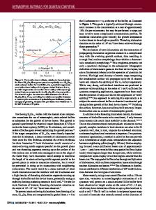
ension of Si CMOS Up until the late 1990s, the performance gains implied by “Moore’s Law”—the number of transistors on an integrated circuit doubles about every node—in microelectronics were achieved mainly through what is now called traditional scaling.1 Roughly speaking, scaling corresponds to shrinking the device dimensions and supply voltage by a constant factor while leaving the materials unchanged.2 The benefits of scaling are increased circuit density, faster devices, and lower power consumption. Note that the performance gains of traditional scaling are not predicated on improvements in materials properties (e.g., channel mobility and gate dielectric permittivity). They are mainly due to reduced capacitance and lower supply voltage. Unfortunately, we are now faced with the reality that fundamental materials limitations make traditional scaling of Si technology problematic. The consensus view is that continued performance improvement requires new materials, new device geometries, and new switching concepts. Replacing Si with high-mobility channel materials (e.g., Ge/GeSn or III–V compounds) (Figure 1) is one near-term approach to improving performance (see the Gupta et al. article in this issue). However, replacing Si and SiO2 is not a trivial task, and complex “integration” issues must be overcome. For example, the lattice mismatch between new channel materials and Si substrates can generate dislocations at the
interface, which degrades performance and yield. To mitigate these effects, graded relaxed buffers,3 dislocation removal,4 and aspect ratio trapping5 to reduce the dislocation density in active areas have all been explored. To date, the performance of these hybrid devices has not matched expectations. For example, while bulk Ge has both high electron and hole mobility (Figure 1), Ge n-channel metal oxide semiconductor field-effect transistors (MOSFETs) do not exhibit the expected mobility enhancement as compared to Si MOSFETs. Currently, III–V (InGaAs) channels are more promising for NFETs. Ge and III–V materials have the appeal that they can be grown on a surface in a similar way as Si, which may make them easier to incorporate in a conventional processing flow. A more radical approach is to use novel one-dimensional (1D) (nanotubes, nanowires) or 2D (graphene, dichalcogenides) nanomaterials in place of conventional semiconductors. Because they are “small,” these materials offer better electrostatic control of the channel, but their integration with conventional processing is potentially very difficult. Finally, devices such as the “tunnel FET” achieve high performance by incorporating new channel materials that enable device switching over a narrow voltage range, and hence with lower power. Moving away from conventional planar devices is another approach to improving performance. Better electrostatic control can be obtained if the gate “wraps around” the channel.
C.W. Liu, Electrical Engineering Department, National Taiwan University, Taiwan; [email protected] M. Östling, School of Information and
Data Loading...