New Method of Computing Band Offsets and Its Application to AlGaN/GaN Heterostructures
- PDF / 331,891 Bytes
- 6 Pages / 414.72 x 648 pts Page_size
- 74 Downloads / 359 Views
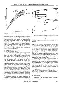
Richard T. Webster* and A. F. M. Anwar** * Air Force Research Laboratory, Hanscom AFB, MA 01730 ** Electrical and Systems Engineering Department, University of Connecticut, Storrs, CT 06269 Abstract Calculated sheet carrier concentration as a function of Al mole fraction in the quantum well (QW) formed at the GaN/AlGaN heterointerface is calculated and compared to experimental data. Close agreement between experiment and theory is observed. The calculated sheet carrier concentration reflects the maximum carrier concentration possible in the GaN QW for a given Al mole fraction and can not be used to argue in favor of either interface charge or piezoelectric effect as giving rise to the carriers. Based on experimental data the charge density in the AlGaN layer is estimated to be 4 x 1012cm- 2 . The calculations are based upon a simple technique to determine valence band alignments. Calculated values are compared to experimental data showing excellent agreement. A calculated valence band discontinuity of 0.42eV for AIN/GaN is well within the experimental bounds. Introduction AlGaN/GaN high electron mobility transistors (HEMTs) are currently being pursued for applications in high power and high temperature microwave circuitry [1-2]. The high bandgap of the GaN channel material allows higher breakdown fields and the low intrinsic carrier concentration allows for better control over free carrier concentration. The low field electron mobility is comparable to that of Si and the peak velocity is close to that of GaAs but occurs at a very high field making it an excellent candidate for high frequency and high speed application as has recently been demonstrated by Khan et. al.[3], Shur et. al. [4], Redwing et. al.[5] and Binari et. al. [1-2] for GaN/AIGaN HFETs. The microwave and the dc performance of the device depends critically upon the behavior of the two dimensional electron gas (2DEG) density and its dependence upon bias and temperature. In this report Schr6dinger and Poisson's equations are solved self-consistently to model the QW. More importantly, a method to determine the valence band alignment is introduced that is extended to include GaN-based heterostructures. Some of the HEMT structures reported by Binari et. al. [1-2] and Redwing et. al.[5] had appreciable two dimensional electron gas (2DEG) concentration though the AlGaN supply layer was undoped. Dangling bonds at the GaN/AlGaN heterointerface may give rise to interface charge that may explain the observed 2DEG concentration. Moreover, charge at the metal AlGaN interface may modify or may be fully responsible for the 2DEG concentration as well. This observation is reminiscent of the Si/Si0 2 technology where charge at the interface created enough band bending so that channel carriers were present at zero bias. Recently, an alternative explanation for the formation of the 2DEG concentration using the piezoelectric effect has been proposed by Asbeck et. al. [6]. In the present paper, theoretical 2DEG concentration is compared to the experimental data from [6] t
Data Loading...