Ni/Si-Based Ohmic Contacts to p- and n-Type GaN
- PDF / 362,044 Bytes
- 6 Pages / 414.72 x 648 pts Page_size
- 14 Downloads / 378 Views
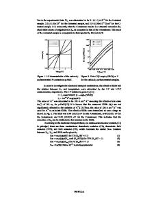
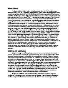
")Institute of Electron Technology, Al.Lotnik6w 46, Warsaw, Poland, [email protected] b)Department of Materials Science and Engineering, North Carolina State University, Raleigh, NC 27695-7907 c)Aixtron AG, Kackertstrasse 15-17, Aachen, Germany d)lnstitute of Physics, PAS, Al.Lotnik6w 46, Warszawa, Poland Olnstitute for Nuclear Studies, Hoza 69, Warszawa, Poland ABSTRACT Ni/Si-based ohmic contact scheme for GaN, based on the solid-phase regrowth (SPR) mechanism have been developed. Using Mg and Si as dopant species, ohmic contacts with a resistivity of -1*10 3fcm2 to p-GaN (p3•3*101 7cm"3) and n-GaN (nz2*10 17cm 3), respectively, have been obtained. SIMS, XRD, and RBS analysis show in as-deposited contacts, an initial reaction at GaN/Ni interface, leading to the formation of an Ni-Ga-N layer. The ohmic behavior of contacts, observed after annealing at 4000C, is accompanied by structural transformations in the contact region: i) the decomposition of Ni-Ga-N layer and ii)the growth of NiSi compound. INTRODUCTION Obtaining low-resistance ohmic contacts to both p- and n-type GaN is one of the big challenges in the production of GaN-based optoelectronic devices such as light emitting diodes and laser diodes. At present, there is only one ohmic contact technology path using (1) low-work function metallizations, such as Ti/At [1,2] for n-type GaN, and (2) high-work function metallizations, such as Ni [3] or Ni/Au for p-type GaN [2,4]. The contacts to n-type material offer suitable electrical properties, with resistivity below 10-5 cm 2 on substrates with doping level of -1017cm3 . Such a low contact resistivity, however cannot be fully explained in terms of Schottky-Mott rule [5], and is attributed to the accumulation of N vacancies, acting as donors, in the vicinity of metal/n-GaN interface, during contact annealing [1,69. In contrast, the resistivity of contacts to ptype GaN is higher by a factor of 103 10 [4]. Since selection of a metal with adequate work function is unlikely to lead to ohmic contact to p-type GaN of required quality, one is led to methods for forming lowresistance contacts by increasing the carrier concentration in GaN subcontact region. From various possible approaches, we have followed the idea of Sands at al. [7] of the incorporation of a dopant into the semiconductor superficial layer by solid-phase dissolution and solid-phase regrowth (SPR). The method relies on the lowtemperature formation, and further reaction driven-decomposition of intermediate phase involving III-V compound. The SPR mechanism has been extensively studied and successfully used to form non-spiking ohmic contacts to GaAs [8-11] and InP [12]; however, no reports on its application to GaN have been published yet. In this paper we report on the development of SPR process to form ohmic contacts to both p- and n-type GaN using Ni/Si contact scheme. We have chosen this 1077
Mat. Res. Soc. Symp. Proc. Vol. 482 ©1998 Materials Research Society
scheme because: (i) Ni is known to penetrate native oxides [4], and to react with GaN alre
Data Loading...