Nickel Determination by Complexation Utilizing a Functionalized Optical Waveguide Sensor
- PDF / 66,725 Bytes
- 6 Pages / 612 x 792 pts (letter) Page_size
- 16 Downloads / 348 Views
Nickel Determination by Complexation Utilizing a Functionalized Optical Waveguide Sensor
Erin S. Carter and Klaus-H. Dahmen Florida State University, Dept of Chemistry, Tallahassee, FL 32312-4390, U.S.A.
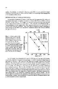
ABSTRACT This research focuses on the design of chemically functionalized optical waveguide sensors. The waveguide is an optically transparent sol-gel coated onto a glass substrate chip. By having a higher refractive index than the substrate, the waveguide internally reflects a laser beam to photodetectors at both ends of the chip. The adsorption of any species onto the waveguide surface changes the light propagation, and therefore its effective refractive index, N. The change in N is dependent upon the amount of analyte present. By covalently bonding specific chemical receptors onto its surface, it can be designed to target a particular analyte. This research involves functionalizing the surface of the waveguide with ED3A in order to complex out of solution Ni2+. The change in N and the thickness of the adlayer will allow the concentration to be determined.
INTRODUCTION The processes that occur at solid surfaces are used in many analytical techniques that involve adsorption and desorption, such as electrochemistry, gas chromatography, liquid chromatography, and capillary electrophoresis. However, the study of surface phenomena is very challenging due to the extremely small quantities of surface-analyte species. Fortunately, a relatively new class of detectors known as optical waveguide sensors (first developed during the early 1980’s by Tiefenthaler and Lukosz at the Swiss Federal Institute of Technology, Zürich) has been used by several research groups to study reaction kinetics at solid/liquid and solid/gas interfaces.[1-4] Optical waveguides are two-dimensional analogs of optical fibers [5]. They are thin (30300 nm), non-crystalline films deposited on an optically transparent glass slide. The simplest waveguide chips are comprised of these two layers- the waveguide and the glass substrate. Because the waveguide has a higher refractive index than the glass substrate, it is possible to pass a plane-polarized laser beam through the substrate onto a diffraction grating inscribed within the chip and ‘guide’ it to a photodiode detector located at either end of the waveguide chip. The refractive index of the waveguide can be determined using the following theoretical relationship (Equation 1): [6] nfilm = sin( αin ) + ( l λ/Λ )
(1)
where nfilm = refractive index of the film, αin =angle of incoupling (angle at which there is total internal reflectance of the laser beam to the detector), l = diffraction order, λ = wavelength of the laser, and Λ = diffraction grating period (2400 lines/ mm). GG9.29.1
The refractive index has been used to determine qualitatively and quantitatively the presence of the compound that is being analyzed. The analysis is carried out by measuring nfilm before and after the waveguide chip has been exposed to a gaseous or liquid medium that contains the analyte. The change in nfilm is depend
Data Loading...