Nitridation Induced-Reactions in Si and SiO 2
- PDF / 961,389 Bytes
- 14 Pages / 420.48 x 639 pts Page_size
- 19 Downloads / 289 Views
NITRIDATION INDUCED-REACTIONS IN Si AND SiO2 RALPH J. JACCODINE Sherman Fairchild Center, Lehigh University, Bethlehem, PA 18015 ABSTRACT Current IC technology uses SiO2 almost exclusively; however, several technological and reliability problems warrant the search for an alternative dielectric. Proposed alternatives are silicon nitride and nitrided Si0 2. This paper reviews the work on thermal nitridation of Si and Si0 2 . Several of the experimental thermal nitridation processes used to achieve good thin dielectrics are discussed. At this time a clear mechanism for the nitridation of Si is not available. The two theoretical attempts to model this process are reviewed. Innovative processes to accomplish the nitridation, such as plasma growth, etc., are presented. Finally, the influence of nitridation on stacking faults and diffusions is also reviewed. I.
INTRODUCTION
The increase in complexity and packing of today's VLSI circuits and projected future trends to even smaller dimensions and tighter packing accentuates the need for thinner insulators with superior dielectrico properties. For example, the 256 kbit DRAM can be produced with -200 f Si02 gate oxides whereas the 1 Mbit DRAM requires insulators more nearly half that thickness. Currently thermally grown SiC2 is the insulator most widely used; however, there are several technological and reliability problems, as the thickness of this insulator is scaled further, that make the search for alternatives warranted. Very thin Si02 films generally have a high defect density causing low field breakdown, the oxide tends to react with electrodes, have poor masking properties with respect to impurity dopants and change charge and trap density when subjected to process and radiation environments [I]. As a result of some of these limitations, a search for alternative thin dielectric material as a replacement for Si02 has been in progress. Thermally grown thin films of silicon nitride have a number of advantages over silicon dioxide. Thermally grown thin films of silicon nitride (direct nitridation of Si) tends to be self limiting and therefore the thickness is easily controllable; however, the range of thicknesses available are limited. Nitride films have high oxidation resistance and even thin coatings are barriers to alkali migration and impurity diffusion and their characteristics do not degrade during VLSI processing [2,3,41. In addition, Si02 films themselves can be subjected to nitridation treatments, with a marked improvement in the properties of the resulting multilayer film [5]. II.
BACKGROUND
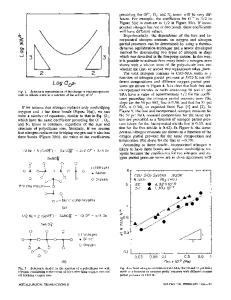
Some of the earliest attempts at growing thermal nitride films for silicon [6) did not succeed in growing homogeneous insulating films because of the influence of oxidant impurities such as water vapor or oxygen in the nitridation ambient. (See Ref. 7 for review.) As can be seen from the calculated stability field diagram for the Si-O-N system, Figure 1, Si N4 can be present in two distinct crystallographic phases, namely alpha-Si N4 and beta-Si 3 N4. The beta phase is s
Data Loading...


