On the nucleation of GaP/GaAs and the effect of buried stress fields
- PDF / 481,268 Bytes
- 6 Pages / 612 x 792 pts (letter) Page_size
- 48 Downloads / 307 Views
0891-EE03-15.1
On the nucleation of GaP/GaAs and the effect of buried stress fields J. G. Zelcovit1, J. R. R. Bortoleto1,3,*,J. Bettini2 and M. A. Cotta1 1 Instituto de Física Gleb Wataghin, DFA/LPD, UNICAMP, CP6165, 13081-790, Campinas-SP, Brazil 2 Laboratório Nacional de Luz Sincrotron, CP 6192, 13084-971, Campinas-SP, Brazil 3 LaPTec, GPM-UNESP, Av. 3 de Março, 511, 18085-180, Sorocaba-SP, Brazil
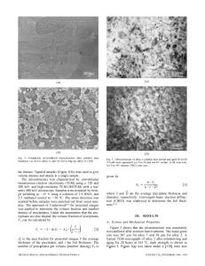
ABSTRACT We have recently shown that spatial ordering for epitaxially grown InP dots can be obtained using the periodic stress field of compositional modulation on the InGaP buffer layer. The aim of this present work is to study the growth of films of GaP by Chemical Beam Epitaxy (CBE), with in-situ monitoring by Reflection High Energy Electron Diffraction (RHEED), on layers of unstressed and stressed GaAs. Complementary, we have studied the role of a buried InP dot array on GaP nucleation in order to obtain three-dimensional structures. In both cases, the topographical characteristics of the samples were investigated by Atomic Force Microscopy (AFM) in non-contact mode. Thus vertically-coupled quantum dots of different materials have been obtained keeping the in-place spatial ordering originated from the composition modulation. INTRODUCTION Epitaxially grown semiconductor nanostructures, using the Stranski-Krastanov growth mode, have an important role in basic research and device applications. In particular, these structures have been grown using epitaxial techniques such as molecular beam epitaxy (MBE) and chemical beam epitaxy (CBE) due to the high degree of control of the film properties they provide. An important aspect in this context is the possibility of obtaining not only control of the size, uniformity and density of these nanostructures, but spatial alignment or ordering as well. [13] . In a previous work, the spontaneous formation of a two dimensional array of self-organized InP/InGaP dots for In-rich coherent InGaP layers was reported [4], caused by compositional modulation[5-13] present on the InGaP buffer layer[14]. In this work, we study the nucleation of both GaP and InAs on GaAs, also using the arrangement of InP/InGaP dots[14]. Previous works[15,16] have shown that the stress field produced by buried islands aligns vertically the islands nucleated in the subsequent layers. Since GaP and InAs have opposite lattice mismatches with regard to GaAs, it would be possible, in principle, to have different vertical correlation (or anti-correlation) to a buried InP dot array if we use different materials in the stack layers. Since InAs growth on GaAs is well characterized in the literature[17-21], we have thus investigated the case of GaP nucleation on unstressed GaAs in order to investigate dot formation. The influence of the stress field created by a template of buried InP/InGaP dots was later investigated by growing InAs and GaP on top of this structure. Our results indeed show the existence of a correlation to the template ordering for InAs and anticorrelation in the case of GaP dots, suggesting that this
Data Loading...