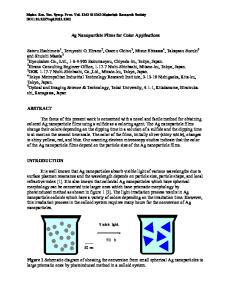
One-Dimensional Ag Nanoparticle Arrays Formed by Decomposition of Precursor Nanowires
- PDF / 754,859 Bytes
- 2 Pages / 576 x 783 pts Page_size
- 60 Downloads / 268 Views
High-Yield Production of Ultralarge Ba0.8Sr0.2TiO3 Capacitors Hinges Upon Pt Dewetting Cracks. Pinholes. Inclusions. Any of these can be a materials researcher’s nightmare foretelling the end to a capacitor. P. Daniels, J. Ihlefeld, W. Borland, and J-P. Maria, however, designed a cost-effective process to develop electrodes that are tolerant of cracks and defects that would normally short circuit a capacitor. Contrary to conventional procedure, they sputter Pt electrodes onto thin-film Ba0.8Sr0.2TiO3 (BST) dielectrics before the annealing process that crystallizes and densifies the ceramic layer. During the 900°C anneal, Pt atoms migrate away from microstructural defects but remain wetted to the rest of the film surface. The researchers from North Carolina State University and Dupont Electronic Technologies say the high-yield process can be used with other oxide–metal combinations to manufacture large-scale, lowcost capacitors. As the researchers describe in their article in the July 2007 issue of the Journal of Materials Research (p. 1763; DOI: 10.1557/
JMR.2007.0272), “Because the probability of depositing an electrode over such a defect scales with capacitor dimension, limitations in yield [traditionally] can be traced to defect area density.” Thus, in the absence of clean room processing, producing millimeter- to centimeter-scale thinfilm capacitors is a tremendous challenge. Using the phenomena of Pt dewetting, the group routinely achieved 5-µF capacitors that were 1 µm in thickness and 2.5 cm in lateral dimension. Functional capacitors had a dielectric loss tangent of < 0.15 (lower values typically mean better quality capacitors). The procedure provides dramatic yield improvement of largescale, functional capacitors without using costly clean room environments and specialized equipment to prevent defects. The success of the procedure hinges upon the naturally high metal–oxide surface energy. Because of the high interfacial energy, thin films of Pt will dewet a dielectric surface at sufficiently elevated temperatures. Daniels and colleagues found that Pt electrodes at least 150-nm thick provide continuous Pt coverage and avoid dewetting and beading during a 900°C anneal.
At this Pt thickness and anneal temperature, however, Pt retreats from the immediate vicinity of cracks or surface asperities, which often lead to short circuit pathways and capacitor failure. The researchers hypothesize that high physical curvature at these potential defect sites drives the electrode rearrangement. The process updates established lowcost fabrication routes to provide highyield, thin-film capacitors. The researchers believe the success of electrode deposition followed by sintering will apply to capacitors with other metal–oxide combinations having high interfacial energy. ASHLEY PREDITH
One-Dimensional Ag Nanoparticle Arrays Formed by Decomposition of Precursor Nanowires Assembling one-dimensional (1D) nanoparticle arrays is more challenging to achieve than generating other nano particle arrays because of their isotropic st
Data Loading...