Nanowires formed in anodic oxide nanotemplates
- PDF / 5,888,138 Bytes
- 5 Pages / 576 x 792 pts Page_size
- 59 Downloads / 419 Views
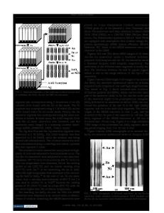
A simple electrochemical method is described for producing metal or semiconductor nanowires with diameters in the continuous range 10 to 200 nm. The technique involves a three-step process that begins with the electrochemical generation of an aluminum oxide template with uniform nanometer-sized pores, followed by the deposition of metal or semiconductor in them. The nanowires are then exposed for study or device fabrication by etching back the oxide matrix. Examples of cadmium nanowires fabricated by this technique are shown.
I. INTRODUCTION Metal and semiconductor films, wires, and particles with small dimensions compared to some critical length can show novel electronic, optical, and chemical behavior due, in many cases, to the confinement of the constituent electrons. This type of behavior has been the recent (and not so recent) subject of numerous theoretical and experimental studies1 that have given rise to picturesque terms such as quantum wells, wires, and dots, and because the effects sought usually occur when the systems' dimensions lie in the 1 to 100 nm range, to expression such as nanowires, nanoparticles, and nanostructures. Of course, one expects (and finds) even more dramatic physical and chemical departures from the behavior of the bulk when dimensions are reduced even further, so that the resulting clusters consist of only a few atoms.2 Nanostructures, however, normally refer to systems where the familiar notions of the bulk such as band gap, conductivity, and so on remain meaningful, but must be modified on account of size. Several strategies have been proposed and applied to the construction of nanostructures ranging from expensive and elegant methods such as molecular beam epitaxy followed by microlithography of ever increasing resolution3 to techniques of arrested aggregation,4 to the use of natural and artificial templates of very small dimensions, the most celebrated of which are the cavities in zeolites.5 One of the commanding goals and challenges in all of this is to create samples with as narrow a size distribution as possible, ideally so narrow that one could use the term monodispersed meaningfully to describe them. In many applications, for example, the development of optically nonlinear materials, it suffices merely to fabricate samples of nanoparticles, which may then be embedded in a suitable matrix. In most electronic and optoelectronic applications, it is also essential to be able to make uniform electrical contact to the nanostructures, 1014 http://journals.cambridge.org
J. Mater. Res., Vol. 9, No. 4, Apr 1994 Downloaded: 26 May 2014
while in the most demanding of applications, it may be crucial to make contact to a single nanoparticle or nanowire. In this report, we present an electrochemical method for producing metal and semiconductor nanowires with a narrow distribution of diameters and continuously variable mean diameters ranging from approximately 10 nm to beyond 200 nm. We also describe techniques for making electrical contacts to the wires for possible electronic and ele
Data Loading...