Optical and Electronic Characterization of a-SiGe:H Thin Films Prepared by a Novel Hollow Cathode Deposition Technique
- PDF / 78,286 Bytes
- 6 Pages / 612 x 792 pts (letter) Page_size
- 30 Downloads / 319 Views
A9.4.1
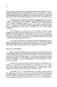
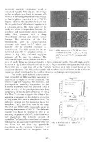
Optical and Electronic Characterization of a-SiGe:H Thin Films Prepared by a Novel Hollow Cathode Deposition Technique R. J. Soukup1, N. J. Ianno1, Scott A. Darveau2, and Christopher L. Exstrom2 1 Department of Electrical Engineering, University of Nebraska-Lincoln, Lincoln, NE 685880511, USA 2 Department of Chemistry, University of Nebraska at Kearney, Kearney, NE 68849-1150, USA Abstract Using a novel hollow cathode plasma-jet reactive sputtering system in which an intense plasma, ignited in an Ar/H2 flow, is directed through silicon and germanium nozzles, a series of a-SiGe:H thin films have been prepared on silicon and glass substrates. These films have been optically characterized by infrared (IR) spectroscopy and spectroscopic ellipsometry (3351000nm). Total hydrogen concentrations, as determined by FTIR, varied with deposition conditions and ranged from 2.5 x 10²¹ to 1.6 x 10²² atom cm-3 and correlated with secondary ion mass spectrometry (SIMS) elemental analyses to within 10%. Conductivity measurements in the dark and under simulated AM1 solar illumination have indicated that the films properties are very good. The light to dark conductivity ratio has consistently been greater than 1000 for films with band gaps down to 1.3 eV. 1. Introduction There is a consensus among researchers that, in order to achieve 15% stabilized efficiency in an amorphous silicon solar cell, a triple-junction amorphous silicon structure is required1. Examples of these high efficiency cells are those described by Deng, et. al.2 and Yang , et. al.3, that consist of a wide band gap a-Si:H cell above a mid band gap a-SiGe:H cell followed by a narrower band gap a-SiGe:H cell. Thus, it can be seen that the a-SiGe:H alloy is a critical component of an efficient amorphous silicon thin film solar cell. The current manufacturing technique for the deposition of thin film amorphous solar cells is plasma enhanced chemical vapor deposition (PECVD)1 employing silane or its derivatives and germane as the semiconductor source gases. Silane is flammable and germane is flammable, toxic, and extremely expensive. The most recent advance in the deposition of a-SiGe:H alloy solar cells is based on the hot wire chemical vapor deposition technique (HWCVD)4-8 in which the films can be grown much faster. Although high quality stable films have been grown at a high rate4,5, the life of the filament is short7 and germane must still be used. The difficulties in working with germane have limited much of the potential basic research on a-SiGe:H alloys, and its incorporation into commercialized cells and modules. In view of this, we have employed a new technique for the deposition of the films to be used to fabricate these solar cells, the hollow cathode plasma-jet reactive sputtering system9-11. This is a germane- and silane-free, high-growth rate technique which can be scaled up to large areas. It is also the only known technique which will allow for the simultaneous, independent control of the deposition of silicon and of germanium. Finally, we have suc
Data Loading...