Optical Characterization of Si Nanowires: Dependence with Substrate Orientation and Light Polarization
- PDF / 7,514,957 Bytes
- 7 Pages / 612 x 792 pts (letter) Page_size
- 115 Downloads / 311 Views
Optical Characterization of Si Nanowires: Dependence with Substrate Orientation and Light Polarization Juan A. Badán1, Ricardo E. Marotti1, Enrique A. Dalchiele1, Daniel Ariosa1, Francisco Martín2, Dietmar Leinen2, José R. Ramos-Barrado2. 1
Instituto de Física & CINQUIFIMA, Facultad de Ingeniería, Universidad de la República, Julio H. Reissig 565, CC 30, CP 11000, Montevideo, Uruguay. 2
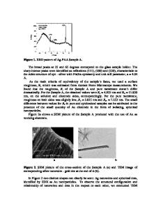
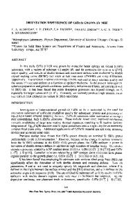
Lab. de Materiales y Superficies (Unidad Asociada al CSIC), Dptos. de Física Aplicada & Ingeniería Química, Universidad de Málaga, Campus de Teatinos s/n, E29071 Málaga, Spain. ABSTRACT Optical properties of Si nanowire arrays (SiNWs) prepared on p-doped Si(111) and Si(100) substrates are studied. The SiNWs were synthesized by self-assembly electroless metal deposition nanoelectrochemistry in an ionic silver HF solution through selective etching. Total reflectance (Rt) and total diffuse reflectance (Rdt) of SiNWs change drastically in comparison to polished Si. To understand these changes diffuse reflectance (Rd) with polarized incident light was studied. For samples prepared on Si(111), the wavelength integrated Rd (wIRd) shows maxima at certain angle of incidence θ and it does not depend on light polarization. Moreover, Rdt of SiNWs prepared on Si(111) can be modeled as an ensemble of diffuse reflectors. For samples prepared on Si(100) wIRd increases with θ, being greater when the light electric field is parallel to the plane of incidence. Also, Rd spectra show structures due to interference effects. For these reasons SiNWs prepared on Si(100) can be considered as a thin film whose refractive index depends on light polarization. INTRODUCTION Silicon nanowire arrays (SiNWs) have important antireflective properties [1]. One reason is their gradual variation of effective refractive index from air to substrate [2,3]. Another one is light trapping by multiple scattering events [2,4], which increases the probability of light absorption [4]. For these reasons their main application is for light enhanced absorption in Si photovoltaic solar cells [5,6]. Another advantage for this application is the possibility of decoupling light absorption and charge carrier collection into orthogonal directions. This condition is satisfied with a junction in the radial direction, and the nanowire (NW) axis parallel to the incident light direction [7,8], e. g. normal incidence of light when nanowires (NWs) are perpendicular to the substrate plane. In this way, the solar cell requirements on the minority carrier diffusion length of the absorber material are reduced significantly in comparison to planar geometry [7-10]. Among the many methods developed for the growth of SiNWs, self-assembly electroless metal deposition (SAEMD) nanoelectrochemistry in an ionic silver HF solution through selective etching is a simple way to prepare SiNWs arrays [11,12]. This method has several advantages with respect to other SiNWs preparation techniques. First, since the as prepared SiNWs are an integral part of the Si wafer substrate, they provide a direct 1D and uninterru
Data Loading...