Dose-window dependence on Si crystal orientation in separation by implanted oxygen substrate formation
- PDF / 1,626,036 Bytes
- 7 Pages / 612 x 792 pts (letter) Page_size
- 45 Downloads / 316 Views
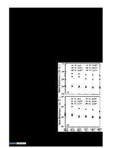
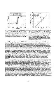
Separation by implemented oxygen (SIMOX)(111) substrates have been formed by oxygen-ion (16O+) implantation into Si(111), showing that a so-called “dose-window” at 16O+-implantation into Si differs from Si(100) to Si(111). In SIMOX(100), an oxygen dose of 4 × 10¹⁷/cm2 into Si(100) is widely recognized as the dose-window when the acceleration energy is 180 keV. For the first time, our work shows that an oxygen dose of 5 × 10¹⁷/cm2 into Si(111) is the dose-window for the formation of SIMOX(111) substrates when the acceleration energy is 180 keV. The difference between dose-windows is caused by anisotropy of the crystal orientation during growth of the faceted buried SiO2. We also numerically analyzed the data at different oxidation velocities for each facet of the polyhedral SiO2 islands. Numerical analysis results show good agreement with the experimental data.
I. INTRODUCTION
The microfabrication technology used in the miniaturization of metal oxide semiconductor field effect transistors (MOSFETs) has played a major role in speeding up and reducing the power consumption of large scale integrated circuit (LSIs). In an era of sub-100 nm MOSFETs, it is difficult to sufficiently improve the operational performance of the devices by merely depending on “scaling laws.” Such materials as gate oxide with high-1 and insulator layers with low-2 have been used to solve this difficult situation for advanced LSI applications. In addition, a new technique that increases the carrier mobility in the channel regions of MOSFETs3 has been investigated for further operational improvement of LSIs. On the other hand, it is true that the above improvements face fundamental limitations so far as electrons are used in transmitting signals. A plan has been unveiled that develops electron-photonmerged devices composed of complementary metal oxide semiconductor (CMOS)-LSI/silicon-on-insulator (SOI) and light-emitting diode (LED)-array/GaN fabricated in the same LSI chip.4 In these devices, electrons and photons are used for computing and signal transfers among LSI chips, respectively. SOI and GaN are used as basic materials for devices at high speeds and at Address all correspondence to these authors. a) e-mail: [email protected] b) e-mail: [email protected] c) e-mail: [email protected] DOI: 10.1557/JMR.2004.0455 J. Mater. Res., Vol. 19, No. 12, Dec 2004
http://journals.cambridge.org
Downloaded: 14 Mar 2015
low power consumption performances, and for optical devices with short wavelengths, respectively. In this case, the orientation of the top Si of the SOI substrate must be (111), i.e., Si(111), because GaN requires 3C– SiC as a suitable buffer material for epitaxial growth, and 3C–SiC is metamorphosed from Si(111).5 Separation by implanted oxygen (SIMOX) technology6 has been investigated to form SOI substrates with Si(111) on top, i.e., SIMOX(111). Although SIMOX(100) substrates with Si(100) on top are commercially available, SIMOX(111) substrates remain undeveloped because no demand exists for such
Data Loading...