Orientation-Dependent Dewetting of Patterned Thin Si Film on SiO 2
- PDF / 1,225,667 Bytes
- 6 Pages / 595 x 842 pts (A4) Page_size
- 12 Downloads / 368 Views
0910-A04-05
Orientation-Dependent Dewetting of Patterned Thin Si Film on SiO2 E. Dornel1, J-C. Barbé1, J. Eymery2, and F. de Crécy1 1 CEA-DRT-LETI, CEA/GRE, 17, rue des Martyrs, Grenoble, 38054, France 2 DRFMC/SP2M équipe mixte CEA-CNRS-UJF, Nanophysique et Semiconducteurs, CEA, 17, rue des Martyrs, Grenoble, 38054, France ABSTRACT The agglomeration of a Silicon On Insulator (001) film during a thermal annealing at 900°C and 950°C under hydrogenated atmosphere has been characterized by Scanning Electron Microscopy (SEM) and Atomic Force Microscopy (AFM). At this temperature, the Si faceting along {110}, {111} and {113} planes is interpreted by a surface energy anisotropy. The anisotropy of the diffusion coefficient is also revealed by the formation of Si line along the , and directions. A mechanism of the pearling instability of the lines is proposed.
INTRODUCTION AND EXPERIMENTAL DETAILS Thin solid films are basic building blocks in microelectronics and optoelectronics. However, due to the shrinking of the layer thickness imposed by technology requirements, the surface to volume ratio increase may lead to morphological instabilities. It has been observed that during a thermal annealing at 900°C during 2 min. (sample A) and at 950°C during 30 min. (sample B) under hydrogenated atmosphere at 20 Torr, a 13 nm Silicon On Insulator (SOI) (001) film can be fully agglomerated in a few minutes. At this temperature (~ 2/3 of the silicon melting temperature), the surface diffusion can be considered as the predominant mass transport mechanism, and the surface energy anisotropy must be taken into account. SEM and AFM have been used to study these samples. The facet orientations of dewetted samples have been analyzed to investigate the morphology evolution and to propose a kinetic mechanism.
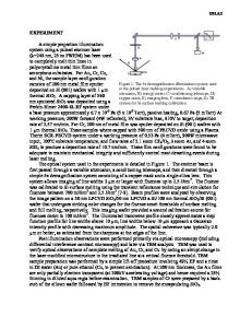
RESULTS AND DISCUSSION Dewetting from the edges of a Si(001) patterned film The system under study is the patterned flat Si thin film on SiO2 shown in figure 1(a). During annealing, the film rearranges in stripes and agglomerates (see figure 1(b)). In agreement with calculations [1,2] and previous observations [3], we observe that the dewetting is initiated from the edge of the pattern. At the beginning of the annealing, the film changes quickly its contact angle α with the substrate to reach the equilibrium Young angle, and slowly smoothes to form a thickened ridge that reduces the surface energy [2]. Figure 2 and figure 3 show an example of thickened ridge of Si on SiO2 parallel to the patterned (a)
tSi = 13nm
(b) Si
Si (001) film SiO2 BOX
22nm over-etch
SiO2 BOX
Figure 1. Sketch of the system under study before (a) and after (b) dewetting.
Figure 2. MEB image of the edge-retraction of a Si film on SiO2 on sample B. The image has been obtained after a local deposition of tungsten assisted by electronic beam to form a protected layer before the focus ion beam (FIB) cutting. The image tilt is 52°. Figure 3. 1.5 µm×1.5 µm AFM image (tapping mode) of the edge-retraction of a 13.8 nm Si film on SiO2 on sample B. The first peak is sl
Data Loading...