Origin of Voids at the Interface of Wafer Bonded Sapphire on Sapphire
- PDF / 9,300,739 Bytes
- 5 Pages / 612 x 792 pts (letter) Page_size
- 60 Downloads / 374 Views
Origin of Voids at the Interface of Wafer Bonded Sapphire on Sapphire
Stephan Senz, Pascal Kopperschmidt and Nikolai Dimitri Zakharov Max Planck Institut für Mikrostrukturphysik, Halle (Saale), GERMANY ABSTRACT Two sapphire (Al2O3, r-cut) wafers were bonded at room temperature. The bonding energy increased during heating up to 1100 °C. The interface was investigated by plan-view and cross-section TEM. The bonding strength after heating to 1100 °C is similar to the bulk bonding strength. A high density of voids at the bonded interface was observed. The voids are elongated along the interface in a pancake shape. The surfaces are low index planes. The volume inside the voids is higher than expected from a model, where a hydrophobic initial bonding is assumed. The strength of initial bonding and the free volume at the interface can be understood, if the sapphire surfaces are hydrophilic and covered by several monolayers of water during initial bonding. During annealing the water diffuses out along the bonded interface and a free volume remains.
INTRODUCTION The improvement of wafer bonding to produce a perfect interface between two single crystals is required for applications like the idea of a compliant substrate. A compliant substrate could operate by gliding of an ideal twist boundary [1,2]. Nevertheless, a general observation after direct wafer bonding of single crystals is the formation of defects at the interface. These defects are most clearly visible, if the bonding is performed at high temperatures or if after initial bonding at room temperature the bonded wafers are annealed. Dislocations at the bonded interface are a result of miscut and relative rotation of the lattices. In some cases defects of several nm size at the interface are observed. These large defects are usually undesired and should be avoided. At the interface GaAs/GaAs or Si/Si they show a white contrast in TEM images, which might be the result either of voids or oxide precipitates. In this paper we present investigations of sapphire wafer bonding, which can be seen as a model system for oxide bonding. Sapphire has the advantage that a clear distinction of voids and oxide precipitates is possible after high temperature annealing. Any precipitate would recrystallize and show no contrast in TEM compared to the single crystal.
EXPERIMENTAL R-cut sapphire wafers of 75 mm diameter were delivered from different suppliers (Union Carbide and CrysTech/Germany) with the best available polishing quality „for epitaxy“. The wafers were not cut exactly with a (1 1 .2) surface. The orientation was checked by x-ray diffraction. The miscut had a random direction and a magnitude of up to 1.5°. Usually the as delivered polishing quality was not sufficient to allow direct wafer bonding. The RMS roughness measured by AFM with a scanning area of 2*2 µm2 should be lower than 1 nm. The required low AA3.19.1
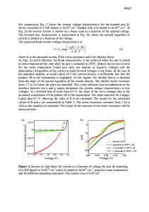
Bonding energy in m J/m
2
4000
3000
2000
1000
0 0
200
400
600
800
1000
1200
Temperature in °C
Figure 1 Increment of bonding energy during heating
Data Loading...