Over 20% Efficiency Mechanically Stacked Multi-Junction Solar Cells Fabricated by Advanced Bonding Using Conductive Nano
- PDF / 241,864 Bytes
- 5 Pages / 432 x 648 pts Page_size
- 37 Downloads / 325 Views
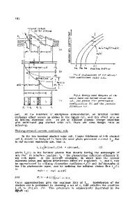
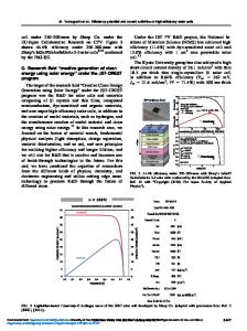
Over 20% Efficiency Mechanically Stacked Multi-Junction Solar Cells Fabricated by Advanced Bonding Using Conductive Nanoparticle Alignments Kikuo Makita, Hidenori Mizuno, Hironori Komaki, Takeyoshi Sugaya, Ryuji Oshima, Hajime Shibata, Koji Matsubara, and Shigeru Niki National Institute of Advanced Industrial Science and Technology (AIST) AIST Tsukuba, Central 2, Umezono 1-1-1, Tsukuba, Ibaraki, 305-8568, JAPAN ABSTRACT This paper shows a new semiconductor bonding technology for mechanically stacked multi-junction solar cells. Our strategy is the combination of conductive nanoparticle alignments and the van der Waals bonding technique. With this method, reasonably low bonding resistances and minimal optical absorption losses were simultaneously attained for the use of mechanically stacked solar cells. We examined a GaInP(Eg-1.89 eV)/GaAs (Eg-1.42 eV)/InGaAsP (Eg-1.15 eV) three-junction solar cell fabricated with this bonding method. As a result, the total efficiency of 22.5% was achieved, which was in good agreement with the theoretically predicted value. These results suggested that our bonding method is highly useful to fabricate high-efficiency mechanically stacked multi-junction solar cells. INTRODUCTION Multi-junction (MJ) solar cells have enabled very high efficiencies due to the effective utilization of the solar spectrum. These MJ solar cells are usually composed of complicated multi-layers on GaAs or Ge wafers using elaborative growth techniques. Therefore, these cells tend to be expensive and lack material flexibility. On the other hand, the MJ solar cells based on mechanical stacking have been considered as an alternative approach to produce MJ solar cells [1-3]. The mechanical stacking enables high efficiency and low-cost because of the flexible combinations of individually-processed cells. We have recently proposed an advanced bonding method using conductive nanoparticle alignments with a simple mechanical stacking process [4,5]. As an initial demonstration, a GaAs(Eg-1.42 eV) / InGaAsP(Eg-1.15 eV) two-junction solar cell was fabricated, and the efficiency of 11.8% was obtained [4]. This efficiency was limited by the small short-circuit current density of InGaAsP bottom cell, because Eg combination (1.42eV/1.15eV) does not meet the current matching. In this report, we design cell structures and cell combinations based on the current matching, and demonstrate a highefficiency (over 20%) for GaInP (Eg-1.89 eV)/GaAs (Eg-1.42 eV)/InGaAsP (1.15 eV) threejunction solar cell. DEVICE CONCEPT Figure 1 shows the schematic drawing of the proposed cell structure, which possesses conductive nanoparticle alignments at the interface between top and bottom cells [4,5]. The conductive nanoparticle alignments were introduced on top of the bottom cell through the use of
167
self-assembled block copolymer (polystylene-block-poly-2-vinylpyridine) templates. As conductive nanoparticle materials, Pd, Ag, Au, and Pt were available. Figure 2 shows the scanning electron microscopy (SEM) image of a typical Pd nanoparticle alig
Data Loading...