Paradox of low field enhancement factor for field emission nanodiodes in relation to quantum screening effects
- PDF / 483,889 Bytes
- 6 Pages / 595.28 x 793.7 pts Page_size
- 77 Downloads / 307 Views
NANO IDEA
Open Access
Paradox of low field enhancement factor for field emission nanodiodes in relation to quantum screening effects Tsung-Chieh Cheng1*, Pai-Yen Chen2 and Shen-Yao Wu1
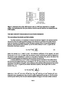
Abstract We put forward the quantum screening effect in field emission [FE] nanodiodes, explaining relatively low field enhancement factors due to the increased potential barrier that impedes the electron Fowler-Nordheim tunneling, which is usually observed in nanoscale FE experiments. We illustratively show this effect from the energy band diagram and experimentally verify it by performing the nanomanipulation FE measurement for a single P-silicon nanotip emitter (F = 4.94eV), with a scanning tungsten-probe anode (work function, F = 4.5eV) that constitutes a 75-nm vacuum nanogap. A macroscopic FE measurement for the arrays of emitters with a 17-μm vacuum microgap was also performed for a fair comparison. Keywords: quantum screening effects, field emission, vacuum electronics, Fowler-Nordheim tunneling, silicon nanostructures
Introduction Recently, micro-/nano-fabricated field emission arrays [FEAs] have attracted a great deal of attention since they have been seen as outstanding electron sources operating with high efficiency, high currents, and fast turn-on times [1-4]. Much effort has been directed toward FEAs’ commercial applications in vacuum electronic devices and components, including vacuum lamps and lighting [5], high-power microwave amplifiers [6], thermoelectric cooler [7], microscopes and visualization equipments, parallel e-beam lithography [8] and, of particular interest, the next-generation flat panel displays [9]. With the rapid advent of nanotechnology, various low-dimensional nanomaterials with extreme aspect ratio and high density, like carbon nanotubes [CNTs] [10], zinc oxide nanowires [11], and silicon carbide nanowires [12], have been successfully fabricated with different synthesis methods, and their excellent field emission properties have been widely reported in the literature. It has been known that field emission [FE] * Correspondence: [email protected] 1 Department of Mechanical Engineering, National Kaohsiung University of Applied Science, 415 Chien Kung Road, Sanmin District, Kaohsiung, 80778, Taiwan Full list of author information is available at the end of the article
properties are highly sensitive to characteristic material properties, like morphology, emitter density, aspect ratio, and electron work function. Among versatile nanomaterials, silicon nanomaterials are of particular interest due to their excellent compatibility to very-large-scale integration [VLSI] integratedcircuit processes. However, the emission currents from conventional FE cathodes with a large vacuum gap, usually larger than hundred micrometers, are insufficient for practical and realistic electronic applications, and the large operating voltages are far too high for being integrated into the standard CMOS electronic devices. However, following Moore’s law for microelectronic devices, within the ever-improving VLSI/US
Data Loading...