Paramagnetic defects in GaN
- PDF / 99,357 Bytes
- 3 Pages / 612 x 792 pts (letter) Page_size
- 18 Downloads / 432 Views
Internet Journal Nitride Semiconductor Research
Paramagnetic defects in GaN M. Palczewska1, B. Suchanek2, R. Dwili˜ski2, K. Paku‚a2, A. Wagner1 and M. Kami˜ska2 1Institute 2Institute
of Electronic Materials Technology, of Experimental Physics, Warsaw University,
(Received Monday, June 22, 1998; accepted Friday, October 23, 1998)
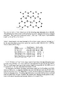
In this work, paramagnetic defects in wurtzite GaN crystals were systematically studied using the Electron Spin Resonance (ESR) technique and using electrical measurements. Three different resonance signals were found. The first had g|| = 1.9514 ± 0.0005 and g⊥ = 1.9486 ± 0.0005, a commonly observed defect in n-type crystals ascribed to the shallow donor of GaN [1]. The second ESR signal, an anisotropic line of g|| = 2.0728 ± 0.0015 and g⊥ = 1.9886 ± 0.0015, was observed only in Mg-doped p-type GaN layers, and was assigned to the Mg acceptor. The last ESR resonance signal, an isotropic line with g = 2.0026 ± 0.0005 was observed only in AMMONO GaN crystals after thermal annealing, as well as in Mg-doped GaN epitaxial layers. It was tentatively identified as due to a deep acceptor.
1
Introduction
The Electron Spin Resonance (ESR) method is a useful tool for identification of defects and impurities in crystal structure. These defects and impurities usually introduce both shallow and deep states in the gap region, and play an important role for electrical and optical properties of semiconductors. Application of gallium nitride (GaN) for blue to near ultraviolet light emitting devices and high-temperature electronics [2] requires an understanding of the nature and properties of both intrinsic and extrinsic defects, and also requires a control of crystal doping. Therefore, we applied the ESR technique for defect studies of GaN crystals grown by different methods. Undoped GaN crystals are typically n-type conductive with carrier concentrations between 1016 and 1019 cm-3. However, the nature of the residual donor has not been positively identified and N vacancies [3] [4], oxygen [5] and silicon [6] have been proposed as possible candidates. Indeed, silicon has been commonly used as the intentional donor dopant up to the 1020 cm-3 concentration range [7], although typical gallium-rich growth conditions of GaN cannot exclude the presence of nitrogen vacancies. Oxygen contamination is also difficult to avoid. As for p-type GaN, magnesium is the only acceptor in GaN crystals so far that can be used to obtain useful p–type conductivity in a reproducible way. However, in as-grown Mg doped crystals obtained by metal
organic chemical vapor deposition (MOCVD), a passivation process plays a crucial role in the compensation mechanism causing creation of neutral magnesium– hydrogen complexes [8]. Therefore, a post-growth treatment is required to activate the Mg acceptors [9]. Mgdoped GaN epitaxial layers obtained by molecular beam epitaxy (MBE) method are p-type without any postgrowth treatment [10] because this technique does not involve hydrogen during growth. In this work, paramagnetic defects in Ga
Data Loading...