Passivation of Silicon Surfaces by Formation of Thin Silicon Oxide Films Formed by Combination of Induction-Coupled Remo
- PDF / 234,389 Bytes
- 6 Pages / 432 x 648 pts Page_size
- 51 Downloads / 320 Views
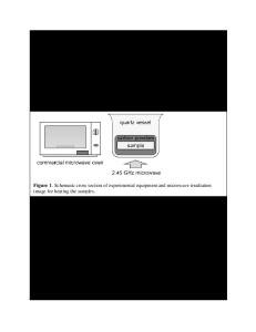
Passivation of Silicon Surfaces by Formation of Thin Silicon Oxide Films Formed by Combination of Induction-Coupled Remote Oxygen Plasma with High Pressure H2O Vapor Heat Treatment H. Abe, S.Yoshidomi, Y. Nagatomi, M. Hasumi and T. Sameshima Tokyo University of Agriculture and Technology, Koganei, Tokyo 184-8588, Japan ABSTRACT We report formation of thin silicon oxide films on the silicon surfaces by combination of oxygen radical and high pressure H2O vapor heat treatment for passivation of silicon surfaces at a low temperature. Oxygen plasma was generated by 13.56 MHz radio frequency inductioncoupled remote plasma with mixed gases of O2 and Ar at 2 sccm, 2x10⁻² Pa and at a power of 50 W. Oxygen radical was produced from the plasma via a metal mesh closing plasma in the reactor. The top surfaces of 20 :cm n-type silicon substrates with the rear surface coated by thermally grown SiO2 layers were exposed by oxygen radical from 1 to 5 min to oxidize the silicon surface. The samples were subsequently annealed with 9.0x10⁵ Pa H2O vapor heat treatment at 260oC for 3 h. The effective minority carrier lifetime estimated using photo-induced carrier microwave absorption system in the case of 635 nm light illumination at 1.5 mW/cm2 to the top surface increased from 1.3x10⁻⁴ to 5.1x10⁻⁴ s as the oxygen radical treatment duration increased from 1 to 5 min. The recombination velocity decreased from 380 to 90 cm/s. 500 kHz capacitance response with bias gate voltages characteristics of metal oxide semiconductor structure resulted in the effective oxide thicknesses (EOT) ranging from 1.3 to 1.7 nm. These results indicate a capability of thin oxide formation and effective passivation of silicon surfaces at a low temperature. INTRODUCTION Semiconductor solar cells have been attractive as a device producing electrical power from sunlight [1,2]. High quality of semiconductors and their surfaces are demanded for achieving a high conversion efficiency of solar cells. Passivation techniques of hydrogen plasma treatment [3, 4] and silicon nitride treatment [5] have been developed. Passivation with thin SiO2 films is also attractive for metal insulator semiconductor (MIS) type solar cells. We recently proposed MIS type solar cells with the top and rear surfaces passivated with SiO2 films [6,7]. Passivation of the both surfaces has an advantage of a long minority carrier lifetime Weff. Thin passivation films are necessary for gathering photo induced current via quantum tunneling effect for the high conversion efficiency. In this paper, we report combination of oxygen radical treatment [8] with high-pressure H2O vapor heat treatment [9] for the purpose of passivation of the silicon surfaces with forming thin oxide layers at low temperature. We report analyses of Weff and the effective oxide thickness (EOT) to discuss passivation of silicon surface at a low temperature. EXPERIMENT 20 Ωcm n-type silicon substrates with a thickness of 520 Pm were prepared. We made two types of samples coated with 100 nm thick thermally grown SiO2 (sample1) and
Data Loading...