Patterning of Microwave Plasma Deposited Diamond Films
- PDF / 1,940,272 Bytes
- 4 Pages / 420.48 x 639 pts Page_size
- 67 Downloads / 454 Views
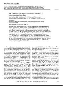
PATTERNING OF MICROWAVE PLASMA DEPOSITED DIAMOND FILMS MOELJANTO W. LEKSONO* AND HOWARD R. SHANKS** *Ames Laboratory-USDOE and Department of Physics, Ames, IA 50011 **Microelectronics
Research Center,
Iowa State University,
Iowa State University,
Ames,
IA 50011
ABSTRACT Patterning has been successfully performed on diamond films deposited on polished silicon wafers from CH4 and H2 gases using microwave plasma chemical vapor deposition. The selectivity was achieved using a lift off process on The lift off silicon wafers which had been polished with diamond paste. process involves deposition and patterning of a thin ZnO film followed by deposition of amorphous silicon using a glow discharge technique. This is The film is deposited followed by microwave plasma CVD of the diamond film. selectively on the crystalline silicon areas of the substrate. Quality and patterning resolution of the resulting diamond films have been determined. INTRODUCTION Diamond has long been recognized to have a unique combination of excellent mechanical, physical, and chemical properties[l]. The recent development of low pressure vapor deposition techniques for the diamond film synthesis including microwave plasma CVD[2-7J has increased the prospects for the practical use of diamond in various forms for applications such as high temperature semiconductor and optical devices[8,9J. For semiconductor device applications selective growth of diamond is essential. There have been several attempts to selectively grow diamond films. Hirabayashi et al.[1O reported selective nucleation of diamond by using Ar ion beam etching on a pretreated substrate which was patterned with resist, while Ma et al.1111 claimed to have more accurate selectivity using oblique irradiation of an Ar beam. In this paper we report for the first time the selective growth or patterning of microwave plasma deposited diamond films performed by a lift off process. EXPERIMENTAL The diamond films were synthesized using a microwave plasma CVD technique[2,5]. A schematic diagram of the system is shown in Fig. 1. CH4 + H2 Power monitor
Substrate
I
tuner
|
a*
2.45 GHz -Microwave Generator
Adjustable short
Waveguide
"Quartz
tube
Fig. I. Schematic diagram of microwave plasma CVD system for diamond films deposition. Pump
Mat. Res. Soc. Symp. Proc. Vol. 189. ©1991 Materials Research Society
88
The microwaves from a 2.45 GHz power supply were guided via a rectangular wave guide through a power monitor and a three-stub tuner to a 27 mm inner diameter quartz tube. An adjustable short was attached to the end of the wave guide and was used to adjust the position of the plasma. The substrate (1.5 cm by 1.5 cm) was put in the center of the quartz tube on a graphite susceptor. For the source of the gas, H2 and a mixture of 5% vol. CH 4 and 95% vol. H2 gases were used. The selective growth was achieved by a lift off process on a polished silicon wafer that can be described in Figs. 2a-c: a. The clean n-type Si(lO0) wafer was polished using 0.25 micron diamond paste, followed by
Data Loading...