PECVD Synthesis of Silicon Nanowires Assisted by Templates of Gallium Islands
- PDF / 1,032,074 Bytes
- 6 Pages / 612 x 792 pts (letter) Page_size
- 7 Downloads / 276 Views
1258-Q04-04
PECVD Synthesis of Silicon Nanowires Assisted by Templates of Gallium Islands Annika Gewalt1, Dr.-Ing. Bodo Kalkofen1, Dr. rer. nat. Marco Lisker2, and Prof. Dr.-Ing. Edmund P. Burte1 1 Faculty of Electrical Engineering and Information Technology, Institute of Micro and Sensor Systems, Otto-vonGuericke University, Universitätsplatz 2, 39106 Magdeburg, Germany 2
IHP GmbH Innovations for High Performance Microelectronics, Im Technologiepark 25, 15236 Frankfurt (Oder), Germany
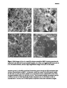
ABSTRACT In this study, we investigated the growth of silicon nanowires forced by small gallium droplet templates. Those gallium islands previously were deposited by a modified PECVD method. Two different delivery techniques of the trimethylgallium precursor (TMGa) were tested regarding their applicability. On the one hand standard liquid delivery was performed, on the other the precursor was transported by vapor draw out of the heated bubbler. The TMGa then was pulsed into the carrier gas flow. The effects on the deposited islands of both delivery methods were compared. As substrates oriented p-doped silicon wafers were used. For the subsequent growth of the silicon wires similarly PECVD was used as growth method. Silane served as precursor. Argon and hydrogen were used as plasma enhanced gases. The effects of the Ga particles deposited by both process modes upon the generated wires were analyzed. INTRODUCTION Silicon nanowires still are one of the favored research subjects, due to the steady miniaturization of electronic devices. There are a lot of future applications, for which only silicon as nano sized material is capable. For example doped silicon wires can be both, a desired and an efficient way out of the pollute electricity generation. To go in detail, an array of silicon wires embedded in a polymer substrate can be used as flexible solar cell [1] which enhances the absorption of sunlight and converts its photons into electrons much better than conventional solar cells. An additive advantage concerning this matter is that only a fraction of the rare high purity semiconductor material will be needed for the production, compared to the amount required for normal solar cells. Additionally, silicon in the form of nano sized whiskers or particles can be used as an alternative to photovoltaic equipment. Because of the explicitly decreased thermal conductivity, in contrast to silicon as bulk material, and thus the correspondent enlarged thermoelectric effect, silicon wires can be used to directly generate electricity out of heat with high efficiency [2]. Last but not least, arrays of identically grown silicon wires can enhance the capacity and durability of lithium ion accumulators, due to the high electrochemical affinity of silicon in regard to lithium as well as the mechanical stability during charge and discharge procedures as result of the flexible array structure [3, 4]. However, to produce reproducible and mass product compliant whisker arrays, there still are some challenges to resolve. To achieve ordered arrays of vertic
Data Loading...