Percolation Conduction of Nanocluster Films for Nano-Devices
- PDF / 720,698 Bytes
- 6 Pages / 612 x 792 pts (letter) Page_size
- 12 Downloads / 290 Views
1257-O03-52
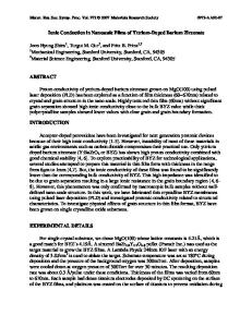
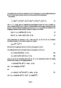
Percolation Conduction of Nanocluster Films for Nano-Devices Il-Suk Kang and Chi Won Ahn National Nanofab Center, Daejeon 305-806, Korea ABSTRACT Electrical conduction of metal nanoclusters by percolation is a very interesting area in nano-device. For more functional nano-sensors consisting of multiple nanocluster blending film, various metals, such as Cu and Ni nanocluster films were fabricated using inert-gas condensation method. The percolation threshold of the films was measured. In addition, for the operation of sensors using these nanocluster films in air, aging experiments of the percolated films in air were carried out. While the percolation threshold was in connection not with the material species but with the area coverage of nanocluster films, the conductive characteristics according to the aging temperature depended on the material species. Reversible and irreversible conduction behaviors of nanocluster films were investigated with nanoscale microstructures using electron microscopes. INTRODUCTION Nanoclusters have possible applications to a wide spectrum of areas, such as advanced materials, electronics, magnetics, optoelectronics, biomedicine, pharmaceuticals, cosmetics, energy, catalytic, and environmental detection and monitoring [1,2]. Electrical conduction of nanoclusters by percolation is also a very interesting area [3-5]. Especially, applications to nonvolatile memory and sensor have been widely studied [6-9]. However, most reported sensors based on percolation use a species of nanocluster. For different chemical sensing capabilities, it is envisioned to go toward multiple nanocluster blending film capable of simultaneously detecting multiple chemical species. For this, percolation conduction of each species of nanocluster requires. In addition, the melting temperature of nanoclusters decreases [10,11]. This property is strongly dependent on the high surface-to-volume ratio, the atomic and electronic arrangement characters, and the size of nanoclusters. Thermal aging of nanoclusters usually causes the irreversible change of electrical resistance because of the competition between oxidation and coalescence or coarsening of clusters. In contrast, the increase of phonon and electron scattering and the tunneling of electron cause the reversible process. In this study, for more functional nano-device consisting of multiple nanocluster blending film, various metals, such as Cu and Ni nanocluster films were fabricated using inert-gas condensation method. The nanoclusters were analyzed by electron microscopes and the electrical conductance of the percolated films of nanoclusters was measured. In addition, for the operation of sensors using these nanocluster films in air, aging experiments of the percolated films in air were carried out and it was demonstrated that the nano-scale morphology with aging process controls the macroscopic properties of these films.
1/6
EXPERIMENT Among processes for the fabrication of nanoclusters [12-17], cluster beam deposition has great potentials because o
Data Loading...