Fabrication Methods for Au Nanocluster Devices
- PDF / 322,081 Bytes
- 6 Pages / 612 x 792 pts (letter) Page_size
- 85 Downloads / 357 Views
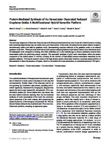
thickness of the shell is determined by selection of the hydrocarbon portion of the thiol [6]. We have synthesized a variety of these clusters where the core diameter varies from 1.3 to 5.0 nm and the shell thickness varies from that corresponding to butanethiol (0.4 nm) to that corresponding to hexadecanethiol (1.0 nm) [7]. For the present work we focus on two of these clusters: The first is designated Au:C6(1:1) and was prepared from a 1:1 HAuCl4:hexanethiol stoichiometry, and the second is designated Au:C2C6(1:1) and was analogously prepared from HAuCl4 and phenethylthiol. To characterize the deposition chemistry of these clusters on SiO2 and on Au we have used XPS and electrical transport measurements. The XPS was performed following depositions on thermally-oxidized Si substrates either with or without a gold coating. The electrical measurements were instead made following depositions on two types of substrates with pre-patterned electrodes, one of micron scale, the other of nanometer scale. The first substrate is a commercially-available gold interdigitated electrode array deposited on a quartz substrate with a chromium underlay (MSI P/N 302 device, Microsensor Systems, Inc.). It consists of 50 finger pairs with a spacing of 15µm, a finger width of 15 µm, a finger thickness of 150nm and an effective total width of 4800 µm. The second substrate was fabricated in-house using standard e-beam lithography with lift-off to create a pattern of Ti/Au finger electrodes on an Si/SiO2 /Si 3 N 4 substrate. These electrodes were single finger pairs with a gap spacing ranging from 12nm to 160nm, a finger width of 50nm and a finger thickness of 30nm. An SEM micrograph of one of the smaller nanofinger devices is shown in Fig. 1. The nitride layer, used to reduce leakage currents, was deposited using plasma-assisted CVD followed by a dry oxidation at 900C. The latter results in the exposed upper surface being SiO 2 and so, from the point-of-view of surface chemistry, it can be presumed to be not much different from the quartz substrate used in the micron-scale devices.
Fig. 1 . SEM micrograph of the nanoscale finger electrode design. alkanethiol functionalization of the substrate is accomplished using an α,ω-alkanedithiol for a gold electrode surface and/or a trimethoxysilane-terminated alkanethiol for the quartz surface. Next, gold clusters are selfassembled on the functionalized surfaces via a substitution
The self-assembly chemistry involves a substitution reaction between a thiol functional group anchored to the electrode or substrate surface and a monothiol- stabilized gold cluster in solution as depicted in Fig. 2. The initial
reaction. Ideally, a continuous layer of clusters would be deposited. In practice, we observe a partial coverage by the clusters.
Fig. 2 . Schematic representation of the gold cluster alkanethiol ligand substitution reaction in the self-assembly deposition process. To obtain a more complete coverage, the initial cluster deposition is activated by treatment with the alkanedithiol for a second s
Data Loading...