Phase diagram and microstructure of microcrystalline and amorphous silicon: a numerical growth simulation
- PDF / 774,304 Bytes
- 6 Pages / 612 x 792 pts (letter) Page_size
- 60 Downloads / 386 Views
A5.3.1
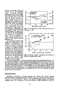
Phase diagram and microstructure of microcrystalline and amorphous silicon: a numerical growth simulation Julien Bailat, Evelyne Vallat-Sauvain, André Vallat and Arvind Shah Institut de Microtechnique, Université de Neuchâtel Breguet 2, CH-2000 Neuchâtel, Switzerland ABSTRACT Growth dynamics and microstructure of thin-film silicon simulated by a 3D dynamical numerical model are investigated. The model, recently introduced, is characterized here with its phase diagram. It reproduces the main features of the growth and microstructure of thin film silicon: amorphous to crystalline phase transition, conical/columnar shape of the conglomerates of nanocrystals, surface roughness evolution of the layer. It is observed that preferential etching of the amorphous silicon is sufficient to reproduce qualitatively the surface evolution observed experimentally. In the presence of preferential etching, nucleation of the microcrystalline phase in the simulated layers always coincides with a surface roughness increase as observed experimentally. This model opens new perspectives for the simulation of thin-film microstructure and surface morphology. INTRODUCTION Hydrogenated microcrystalline silicon (µc-Si:H) prepared from a silane and hydrogen gas mixture, by plasma-enhanced chemical vapor deposition (PECVD), is a promising material for large-area thin-film solar cells [1] and thin-film transistors (TFT) [2]. An improved control of the growth of the material is necessary in order to optimize these microcrystalline devices. Consequently, their microstructure [3] and growth dynamics [4] are currently being intensely studied and simulation tools for the prediction of the layer microstructure are desirable. For metallic layers used in very large scale integration, a growth model is used to predict the layer topography grown on top of the high aspect ratio structures [5]. For thin-film silicon deposited by PECVD, a 3D dynamical discrete growth model introduced by the authors in a previous contribution [6], allows for the qualitative prediction of the surface morphology and microstructure of microcrystalline silicon. This model is able to reproduce the experimentally observed phase transitions from amorphous to microcrystalline material, with respect to the silane concentration and to the accumulated film thickness [7]. The simulation is based on two simple selection rules: • First rule: After random deposition and local relaxation of a particle on the growing surface, a crystallographic orientation is attributed in such a way, that the relaxing particle tends to be in the same crystallographic orientation as its neighbors. This self-organization process is responsible for the growth of conically shaped crystalline domains, similar to those experimentally observed in µc-Si:H. • The second rule allows for the removal of the deposited particle (desorption). This is implemented in such a way as to preferentially remove the particles belonging to the amorphous phase. Two of the three model parameters are related to the material proper
Data Loading...