Photo-CVD of Dielectric Films by a Microwave-Excited VUV Lamp
- PDF / 1,484,184 Bytes
- 8 Pages / 417.6 x 639 pts Page_size
- 20 Downloads / 259 Views
PHOTO-CVD OF DIELECTRIC FILMS BY A MICROWAVE-EXCITED VUV LAMP
KOUICHI TAMAGAWA, TOSHIO HAYASHI AND SOUJI KOMIYA ULVAC Corporation, Chigasaki, Kanagawa 253, Japan
ABSTRACT Silicon nitride and oxide films have been formed using a photo-CVD apparatus with a microwave-excited VUV lamp. The lamp used was a D2 lamp or For the nitride film a rare gas resonance line lamp such as Xe and Kr. 0 deposited at 320 C, the BHF etching rate of the film, 40-70X/min, is lower by less than one-tenth than that deposited using a conventional low-pressure Hg lamp, indicating formation of a high density film. The deposition rate has been enhanced dramatically from 13A/min to lOOA/min by incorporating the photo-ionization assisted effect, which is brought about by an ionization of a substrate surface and by ions formed by collisions of reactant gases with photoelectrons and photo-ionized ions. The BHF etching rate of the oxide film is considerably lower than those formed using a Hg lamp and excimer lasers, and is similar to that using conventional PE-CVD. Conformal step coverage has been obtained for both the silicon nitride and oxide films.
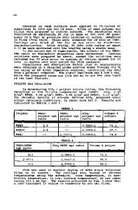
INTRODUCTION There is considerable interest in low-temperature semiconductor fabrication processes. Low-temperature processes are a critical requirement since high-temperature processes cause wafer warpage, dopant redistribution, and defect generation and propagation. Photochemical vapor deposition (photo-CVD) is the most promising candidate for the low-temperature process, and materials such as crystalline Si [1,2], amorphous Si:H [3,4], SiOx:H [57], SiNx:H [8-10], many kinds of metals [11,12] and compound semiconductors [13-15] have been deposited by photo-CVD. In many studies, commercially available low-pressure Hg lamps and excimer lasers have been employed; however, photon energies, about 4 to 7eV, of these light sources are in some cases not sufficient for dissociating reactant gases and/or enhancing surface migrations of adsorbed species. Indeed, densities of dielectric films such as silicon nitride and oxide formed by photo-CVD are commonly known to be low and, therefore, etching rates of these films are much higher than those formed by high-temperature CVD (HT-CVD) and are considerably higher than films by plasma enhanced CVD (PE-CVD) [7,9,16,17]. High energy vacuum ultraviolet (VUV) photons (-lOeV), in contrast, provide several advantages for the photo-CVD process: (1) the absorption cross section of many reactant gases increase with decreasing wavelength in the VUV region, and (2) these photons can not only dissociate reactant gases efficiently but also ionize parent and photo-dissociated gas species, and/or a substrate surface through emission of photoelectrons. In this study, we demonstrate that high density silicon nitride and oxide films have been formed by photo-CVD. In the nitride film deposition dramatic enhancement of the deposition rate by means of the photo-ionization assisted effect is also Table I. Ionization potential of demonstrated. A photo-CVD molecules and radicals(eV). a
Data Loading...