Photolithographic Patterning of Vacuum-Deposited Organic Light Emitting Devices
- PDF / 1,996,585 Bytes
- 6 Pages / 414.72 x 648 pts Page_size
- 57 Downloads / 335 Views
593
Mat. Res. Soc. Symp. Proc. Vol. 488 © 1998 Materials Research Society
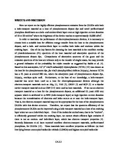
patterned using a second mask consisting of 400 grm x 1 cm strips centered over the holes in the /Photoresist Si
OLED layers
2
Yolyim ide
i
:
ITO
:
(a):U ndercut formation
(b): Norm al incidence
evaporation of OLED layers
~~I a
Metal Cap
(d):Lift-off
(c): Oblique incidence evaporation of protective metal cap
Figure 1. Schematic diagram of steps used in the photolithographic patterning of vacuum-deposited, small molecular weight OLEDs polyimide layer. Undercuts were formed by wet etching the SiO 2 layer (Fig. Ia). Next, the OLED layers were evaporated in vacuum under a base pressure of 3 x 10.6 Torr through the photoresist patterns in a direction normal to the substrate plane (Fig. Ib). The growth sequence was: 1) a 400A thick a-NPD hole transport layer; 2) a 600 A thick Alq 3 layer serving as both the light emitting and electron transport material; 3) a 250 A thick Mg:Ag cathode co-evaporated with an atomic ratio of 24: 1; 4) a 200 A thick Ag protection layer. Next, a 0.5 lan thick Ag layer was obliquely deposited onto the substrate to cover one side of the devices (Fig. 1c), followed by rotating the substrate 1800 and evaporating a second 0.5 lrm thick Ag layer to cover the opposite side of the devices. This process can be simplified by installing a planetary mount into the vacuum chamber which allows for substrate rotation during deposition. Finally, lift-off of the photoresist mask was done by soaking in acetone for several minutes, followed by drying in pure N2 (Fig. Id). A more detailed description of the process can be found in Ref. 15. RESULTS
300 lim
100 grm
OLED
SiO
2
Figure 2. Photograph of seven completed, photolithographically patterned devices. The overall smooth appearance of the devices shown in Fig. 2 indicates no obvious solvent penetration into the organic materials due to the encapsulation by the Ag caps. A few defects, possibly
594
caused by particles preexisting on the substrate, or introduced during subsequent film deposition, can be eliminated by proper handling in a suitably clean environment. Figure 3 shows the forward biased current-voltage (I-V) characteristics of the devices before and after lift-off. The inset shows the electroluminescence (EL) spectrum of a device after lift-off. Both the IV characteristics and EL spectrum are similar to those previously reported for conventional devices 10.
,o olo \ o015
10-6
-0
10-
o
Before lift-off After lift-off
0.10
V
"I
0.005l
10-1 10
1 .1
00.]
A
10'1e
10. 13 0.1
1 Voltage (V)
10
Figure 3. Current vs. voltage characteristics of a 0.45rmm2 device obtained prior to and after photoresist lift-off in acetone. Inset: Electroluminescence spectrum of the patterned device. fabricated by shadow mask techniques[16]. We note that a few devices were shorted before lift-off, possibly due to metal bridges causing shorts between the metal on the photoresist surfaces and the device caps. After lift-off, however, all devices were electrically iso
Data Loading...