Photoluminescence Characterization of p-type GaN:Mg
- PDF / 384,001 Bytes
- 6 Pages / 414.72 x 648 pts Page_size
- 88 Downloads / 223 Views
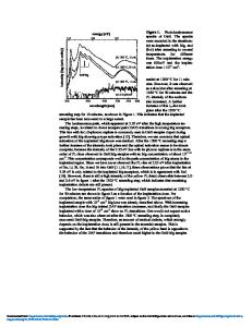
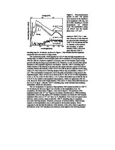
ABSTRACT We report on results of low-temperature photoluminescence measurements performed on GaN films, grown by molecular beam epitaxy (MBE) on sapphire substrates. The GaN films are either Mg doped (p-type) or consist of a Mg-doped layer on top of a Si doped GaN layer (n-type). In the p-doped samples, the sharpness of the donor-acceptor-pair transition is striking, three phonon replicas are clearly resolved. A transition band occurs around 3.4 eV, which becomes dominant for samples with an np-layer structure. The position and the composition of the near band edge transitions are influenced by the growth of the buffer layers. Depending on the growth conditions a transition at 3.51 eV can be observed.
INTRODUCTION The interest in GaN for application hi optoelectronic devices, i.e., light-emitting diodes, has rapidly grown in recent years. The performance of the pn-junction of a diode is strongly related to the quality of the doped layers. Furthermore it has been shown [1,2] that stress, which is caused by the lattice mismatch between layers and substrate, by differences in thermal expansion coefficients and point defects, has a significant influence on the optical properties as well as on the doping properties [3]. In this respect investigations have shown that the growth of the buffer layer plays an important role in strain engineering [1,4]. The systematic control of the strain becomes more complex with increasing number of different layers. Mg is nowadays commonly used as a p-type dopant [5] but still the properties of GaN:Mg are not fully understood. The incorporation of Mg depends also on strain and stress present in the film [3], which is determined by the buffer layer. In order to study this influence, p-type and np-type structures were grown on top of different buffer layers.
EXPERIMENTAL The GaN samples under investigation are MBE-grown using a Riber 1000 chamber. Ga, Mg and Si are evaporated from Knudsen cells and the activated nitrogen is provided by a CGD plasma source [6]. To guarantee a homogeneous heat distribution, a thin titanium (Ti) layer is evaporated on the back of the sapphire substrates. First the substrate is nitridated at around 700 TC and then a thin GaN buffer layer with a typical thickness of 20 nm grown at 500 TC is deposited on it. Subsequently the main epitaxial GaN layer is 673 Mat. Res. Soc. Symp. Proc. Vol. 482 © 1998 Materials Research Society
grown. Typical growth conditions are: Ga source temperature 1210 K, N flow rate 5 - 80 sccm. For this study the MBE growth process of Mg doped GaN, grown directly on the buffer layer, was optimized in order to gain high Mg incorporation and p-type mobility (sample P1 of Table 1). Furthermore a set of np-structures was produced. The thicknesses and the growth conditions of the buffer layers were varied. On the buffer layer first a Si doped GaN film (n-type) and subsequently a GaN:Mg film (p-type) was grown. The following table gives an overview of the studied samples. Table 1: Growth parametersof the samples under investigation. name P1 N
Data Loading...