Photoluminescence characterization of Mg implanted GaN
- PDF / 64,396 Bytes
- 7 Pages / 612 x 792 pts (letter) Page_size
- 9 Downloads / 446 Views
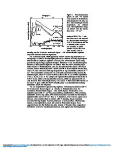
owever, depending on the crystalline quality of the sputtered AlN, good results were obtained only for some selected samples [6,10]. In this article we present results on the basis of an improved annealing technique. Instead of polycrystalline AlN-cap layers, we used thin AlN layers epitaxially grown on top of GaN-samples to protect the GaN surface from decomposition during annealing after the ion implantation of Mg. Magnesium was used because of its known behavior in GaN and the well known corresponding PL signatures. EXPERIMENTAL One-to-two µm thick epitaxial, monocrystalline and nominally undoped GaN films were grown on on-axis n-type, Si-face α(6H)-SiC(0001) substrates at 1000 oC and 45 Torr using a vertical, cold-wall, RF inductively heated MOVPE deposition system [12]. High-temperature (1100 °C) mono-crystalline AlN layers were deposited prior (100 nm) and following (30 nm) to the GaN growth. Deposition was performed using triethylaluminum (TEA) and triethylgallium (TEG) in combination with 1.5 SLM of ammonia (NH3) and 3 SLM of H2 diluent. Magnesium was implanted with ion energies of 60 keV or 120 keV at room temperature. TRIM simulations gave a mean ion range of 70 nm (FWHM = 40 nm) and 127 nm (FWHM = 101 nm), respectively, for the two energies [13]. Thus, the implanted magnesium ions penetrated the AlN-cap layer in both cases, which was also experimentally checked and confirmed by SIMS measurements. The total implantation dose ranged between 1013 cm-2 and 1015 cm-2. All implanted samples were annealed under vacuum (< 1.104 mbar) up to temperatures of 1300 °C for 10-30 minutes. The AlN cap layer inhibited surface decomposition of the GaN sample. Photoluminescence measurements (PL) were performed after each annealing step at low temperatures by exciting the GaN samples with a He-Cd laser (3.81 eV). The AlN-cap layer was removed by dry etching in an ICP plasma (300 W, bias: 10 V, 30 sec.) [14]. Hall measurements were done in Van-der-Pauw geometry after the deposition of Pd(50 nm)-Au(100nm) contacts at a rate of 0.1-0.2 nm/s and 6.10-6 mbar. RESULTS AND DISCUSSION The low temperature PL spectra of Mg-implanted GaN with a dose of 1.1013 cm-2 are summarized in figure 1 as a function of annealing temperature and time. No PL lines were observed directly after ion implantation, which indicates a highly disturbed GaN lattice. This behavior was, of course, also observed for the higher implantation doses used in this study. The high defect density introduced into the crystal by the ion implantation process leads to non-radiative recombinations of the excited electrons with holes; thus, no luminescence is visible. Intense PL lines have been detected after annealing the Mg implanted GaN sample at a temperature of 1200 °C for 11 minutes (see figure 1(b)). However, the intensity of the band edge luminescence is still about 2-3 orders of magnitude lower in comparison to asgrown, unimplanted GaN samples. This luminescence line at 3.467 eV (commonly labeled as I2) originates from recombinations of excitons bound to shallow dono
Data Loading...