Polymer Used for Semiconductor and Dielectric in Photosensitive FET
- PDF / 146,883 Bytes
- 1 Pages / 576 x 783 pts Page_size
- 20 Downloads / 373 Views
use of an alloy-ceramic oxide multilayer. The optical performance of these multilayers in the water-window soft-x-ray region is anticipated to be better than in the hardx-ray region due to the decrease in diffuse scattering from high-frequency roughness at longer wavelengths. IULIA MUNTELE
Polymer Used for Semiconductor and Dielectric in Photosensitive FET K.S. Narayan and N. Kumar from Jawaharlal Nehru Centre for Advanced Scientific Research in Bangalore have fabricated a field-effect transistor (FET) which consists of a polymer semiconductor and a polymer dielectric layer along with metal contacts. The researchers reported in the September 17 issue of Applied Physics Letters that this FET responds dramatically to light and controls the transistor properties. The researchers used poly(vinyl alcohol) (PVA) as the transparent, insulating medium and cast it on a glass substrate coated with a partially transparent (10%) gate aluminum electrode to form a micron-
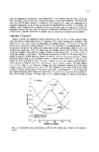
thick layer. They dissolved regioregular poly(3-octylthiophene-2,5-diyl) (P3OT), with 98.5% head-to-tail regiospecific conformation, in chloroform and spin-coated on the insulator to form a 100-nm-thick film. The source and drain electrodes were formed with 3-mm-wide gold electrodes with an interelectrode spacing of 70 µm. The transistor exhibits large photosensitivity represented by sizable changes in the drain-source current at low levels of light, according to the researchers. They reported a current gain of ≈ 100 for a photon flux rate of ≈ 1 µW. They reported that the current gain could be increased to as high as 103 with higher flux rates and a 150-nm-thick layer of P3OT. They observed that the threshold of the drain source voltage needed to drive the drain current to saturation decreased with increasing light intensity. The researchers said the light-responsive polymer FET opens a new device-architecture concept for polymer-based electronics as image sensors. “The salient feature in this device is that both the active and dielectric media are polymers. This feature
can enable fabricating circuit patterns using processing routes such as ink-jet printing and soft lithographic procedures,” said Narayan.
Semiconductor Reservoirs Serve as Sources of Coherent Spin Current Researchers at the University of California—Santa Barbara (UCSB) and the Pennsylvania State University have discovered a persistent mode of spin current deriving from semiconductor reservoirs that serve as a source of coherent spin currents. In their study reported in the June 14 issue of Nature, they have demonstrated high-efficiency spin transfer through interfaces between n-GaAs/n-ZnSe as well as between p-GaAs/n-ZnSe under external electrical bias. David Awschalom, director of the UCSB Center for Spintronics and Quantum Computation and head of this research team, said that previously, theories of electron transport from one material to another suggested that the spin would lose its orientation or scatter from impurities or structural effects. In this study, the spins of
◗ papers publ
Data Loading...