Porous Organosilicates for On-Chip Dielectric Applications
- PDF / 1,915,749 Bytes
- 13 Pages / 417.6 x 639 pts Page_size
- 44 Downloads / 328 Views
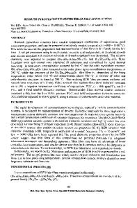
decreases in wiring dimensions and pitches. The calculated RC delays of the interconnects depend on the resistivity of the metal lines, and the dielectric constant of the on-chip insulators as well as the length and pitch of the wiring interconnects) As shown in Figure 1, increasing the wiring densities will trigger unwanted increases in signal delay unless accompanied by simultaneous decreases in metal resistivity and/or the dielectric constant of the insulating media. Figure 1 shows the calculated signal delays for AI(Cu) and Cu interconnects and the current silicon dioxide insulator (k = 4.0) versus those of a hypothetical material with k = 2.0. Recently, reliability studies on multilevel devices prepared in a manufacturing environment demonstrated that traditional aluminum/copper wiring may be replaced by copper, resulting in an approximately 40% decrease in the metal interconnect resistivity,3 and it is clear that this innovation will be incorporated in future advanced devices.4 This alone, however, will not sustain the proposed scaling of future devices without subsequent decreases in the dielectric constant of the insulator. Realization of lower dielectric constants in the interconnect insulators will also improve power consumption, an additional chip performance issue. It is clear that in order to maintain scaling in future devices, simultaneous advances will be required in many areas including device design, lithographic processes, metal interconnect resistivity and dielectric insulators. While innovative approaches to the first three issues have progressed, it is clear that materials research on low k insulators has lagged somewhat behind.
... * Gate delay 40
Sum of delays, AJ&S0 2 of delays, Cu and Low k Interconnect delay, Al & SlO2 Interconnect delay, Cu & Low k
-
-A-
4
-Sum
----
35 30
" -6
4-
-
-
S20AL
Al Cu S102
3.Opil)-cm 1.7giL-cm k = 4.0
Low k
k = 2.0 0.8i Thick
"&25 &Cu
•wt. Ad&S0/A s
Gat
_
/
43V Long
AI&Cu Une
•.•
/ /
,
:
I
Gate w
/
Gate -/
Cu&
.*
10
650
500
350
250
180
130
100
Device Generation (nm)
Figure 1: Calculated delays for aluminum and copper interconnects. This situation is exacerbated by the daunting materials requirements resulting from the long-term, systematic optimization of semiconductor integration criteria based on silicon dioxide insulators. Progress in new dielectrics is further complicated by the uncertainty of whether advanced dielectric insulators will be deposited by vapor phase deposition (CVD) techniques or will be applied by solution spin-on procedures. The former has a long and successful history, but seems to suffer from uncertain extendibility to ultra low k materials (k < 2.2). The latter, in spite of its track record for photoresists, has raised some questions in applications to on-chip dielectric insulators. What seems clear, however, is that switching back and forth between different deposition techniques for new device generations is not an attractive option. In spite of the uncertainty regarding the preferred method f
Data Loading...