Preparation and Characterization of Rare Rarth Scandate Thin Films as an Alternative gate dielectric
- PDF / 865,426 Bytes
- 6 Pages / 612 x 792 pts (letter) Page_size
- 87 Downloads / 471 Views
0917-E05-10
Preparation and Characterization of Rare Rarth Scandate Thin Films as an Alternative Gate Dielectric M. Wagner1, T. Heeg1, J. Schubert1, St. Lenk1, C. Zhao2, M. Caymax2, and S. Mantl1 1 Institute of Thin Films and Interfaces, Research Centre Juelich, Leo-Brandt-Strasse, Juelich, NRW, 52428, Germany 2 IMEC, Kapeldreef 75, Leuven, 3001, Belgium
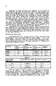
ABSTRACT Rare earth scandate thin films (GdScO3 and DyScO3) were investigated with respect to future high-κ applications. They were deposited on (100) silicon substrates using either pulsed laser deposition (PLD) or electron beam evaporation. The investigation of the films was done by means of Rutherford backscattering spectrometry, high-temperature X-ray-diffractometry, X-ray reflectometry, spectroscopic ellipsometry, transmission electron microscopy (TEM) and atomic force microscopy. For the electrical characterization capacitor stacks were prepared. Both materials show very promising characteristics independent from the deposition technique used. The films are stoichiometric and amorphous and exhibit a smooth surface (roughness RMS < 1 Å). The amorphous phase is stable up to 1000°C. The electrical characterization revealed featureless C-V-curves with a small hysteresis. From CET plots (CET = capacitance equivalent thickness) κ-values between 20 and 23 could be extracted. The electron beam evaporation produces films with a better homogeneity and a thinner interfacial silicon dioxide and therefore a smaller CET value as confirmed by TEM. The leakage current density of the film with CET = 1.5 nm was as low as 7.7x10⁻⁴ A/cm². INTRODUCTION In order to increase the performance of integrated circuits all the dimensions of the microelectronic devices have to be scaled down including the thickness of the insulating gate oxide between the gate electrode and the conducting channel of a silicon based MOSFET. But as the conventionally used silicon dioxide film reaches a thickness of below 1 nm the tunneling current through the film starts to rise exponentially causing an intolerable power dissipation and finally the thermal breakdown of the device. A solution to this problem is the substitution of the silicon dioxide with a so-called high-κ material which high dielectric constant allows to increase the film thickness of the gate oxide again while preserving the same gate control of the MOSFET. Therefore the International Technology Roadmap for Semiconductors [1] explains the integration of high-κ dielectrics in the CMOS process to be one of the major challenges in the near future. During the past years many candidates for high-κ-dielectrics have been investigated like Si3N4, Al2O3, ZrO2, LaAlO3, SrZrO3 or HfO2 [2] but none of them seems to meet all the requirements. These are a sufficient high permittivity, large bandgap and band offsets, thermodynamic stability in contact with silicon up to 1000°C, a good film morphology, a high interface quality, compatibility with other materials used in the CMOS process and with the process itself and the long term reliability of the fi
Data Loading...