Preparation and Characterization Silver and Copper Layers on Polyimide Prepared by Electroless Copper Plating
- PDF / 1,231,167 Bytes
- 7 Pages / 612 x 792 pts (letter) Page_size
- 58 Downloads / 425 Views
0947-A03-05
Preparation and Characterization Silver and Copper Layers on Polyimide Prepared by Electroless Copper Plating Eun Sun Ji, Young Hwan Kim, and Young Soo Kang Department of Chemistry, Pukyong National University, 599-1, Daeyeon 3-dong, Namgu, Busan, 608-737, Korea, Republic of
Preparation and Characterization Silver and Copper Layers on Polyimide Prepared by Electroless Copper Plating
Eun Sun Ji, Young Hwan Kim and Young Soo Kang* Department of Chemistry, Pukyong National University, 599-1 Nam-gu, Busan 608-737, Korea*
Email: [email protected]
ABSTRACT Ag particles were generated on Ag+-doped polyimide film by ion exchanging, followed by copper deposition using metallic silver particles as seeds. The Cu layers were coated on the surface of polyimide films by electroless plating method. The surface image and morphology of Cu layers on the polyimide films were characterized with scanning electron microscopy (SEM), and atomic force microscopy (AFM). The chemical composition on the PI film was investigated energy dispersive X-ray (EDX) spectrometer.
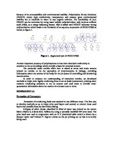
INTRODUCTION Most polymeric materials are transparent to electromagnetic radiation and provide no shielding against electromagnetic interference (EMI). In electronics and communication industries, the EMI pickups by electronic components raise serious problems such as noise enhancement and malfunction of electronic instruments. Accordingly, EM shielding has been the topic of much research in recent years [1,2]. Although, many EM shielding methods are available for electronic plastic packaging, not many methods are available for optical-electronic plastic packaging. Low cost, high EM shielding optical laser modules made with the modified thermosets using compression molding technology were reported [3,4]. Copper can have the electromagnetic wave shielding, and so has become a preferred choice for the microelectronics industry. To further increase the electromagnetic wave shielding, the use of an insulating medium with a low dielectric constant (low-k) material is necessary. Hence, the combination of Cu-based metallization and low-k materials is a good solution for the microelectronics industry. Polyimide (PI) has been increasingly used in the microelectronic packaging industry. Polyimides are generally characterized by excellent thermal, chemical, and mechanical stability and low-k. Various efforts have been made to produce metallization on PI surface. Copper electroless metal deposition is a primary choice because it is a relatively low-cost and lowtemperature technology. In several of these applications, deposition of a metal layer on PI substrates is necessary step to creating an electrically conducting via or interconnections. However, due to the somewhat inert surface of PIs, it is difficult to form adhesive bonds with these materials. If the desired bulk properties of PIs are to be retained then an alternative to this problem is surface modification [5-7]. There are numerous methods for performing metallization on the PI films. In addition to the physic
Data Loading...