Properties of A-(Si,Ge) Materials and Devices grown using Chemical Annealing
- PDF / 269,332 Bytes
- 6 Pages / 432 x 648 pts Page_size
- 41 Downloads / 262 Views
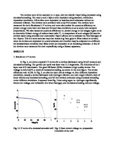
Properties of A-(Si,Ge) Materials and Devices grown using Chemical Annealing Ashutosh Shyam, Daniel Congreve, Max Noack and Vikram Dalal Iowa State University, Dept. of Electrical and Computer Engr. and Microelectronics Research Center, Ames, Iowa 50011 ABSTRACT Chemical annealing is a powerful technique for controlling H bonding and optical absorption in amorphous semiconductors. We have shown previously that the use of careful chemical annealing by Argon can lower the bandgap of a-Si:H while maintaining electronic properties in both films and devices. In this work, we describe new work on chemical annealing of A-(Si,Ge):H films and devices. The technique consists in growing very thin layers (1-3 nm) of A-(Si,Ge) from mixtures of hydrogen, Silane and Germane, and then subjecting this thin layer to ion bombardment by Ar. The cycle is repeated many times to achieve the desired thickness of the intrinsic layer. The resulting film and device were measured for their composition using energy dispersive spectroscopy (EDS) analysis. We discovered that the composition itself, namely the Ge:Si ratio in the film, could be varied by changing the ion bombardment conditions. Lower energy bombardment led to a higher Ge:Si ratio for the same germane/Silane ratio in the gas phase. By controlling ion bombardment during the Ar annealing cycle, we were able to reduce the H content of the film and achieve good electronic properties. It will be shown that by appropriate control over ion energies, one can obtain films and devices which are of good quality and low bandgap as well. INTRODUCTION A-SiGe is an attractive candidate for low bandgap material. However owing to its poor electronic properties it presents considerable challenge in fabricating high quality solar cell. This study is dedicated to the fabrication of low bandgap, but high quality solar cells using A-SiGe. In our previous work[1] we had shown that it is possible to fabricate high quality ( FF ~ 65%), low bandgap ( Eg~ 1.62 Ev) device using a layer by layer approach, which is also known as chemical annealing[2,4] in which a thin layer of A-Si was grown ( ~10Å) followed by Ar Ion bombardment. The objective of this study is to try and apply the same technique to A-SiGe. We have on one hand, focused on effect of ion bombardment of Ar on material property and bandgap, and on the other hand discussed the effect of RF power on the Ge content of devices. It has also been shown that it is vital to compare bandgaps of continuously grown or non annealed (NON CA) and chemical annealed (CA) devices with identical Ge-Si composition. Mainly p-i-n devices and films were studied for the purpose of this study. EXPERIMENTAL DETAILS The growth of devices was done using PECVD growth technique, in which frequency used was in the VHF range, ~ 45 MHz. The growth temperature was about 275C. The growth was
229
done using a mixture of Silane, Germane, Hydrogen and Argon, and the annealing was done using just Argon. For comparison we used devices with the same SiGe composition as chemically annea
Data Loading...