Properties of RF Sputtered ZnTe:N films for Back Contact to CdS/CdTe Solar Cells
- PDF / 57,979 Bytes
- 6 Pages / 612 x 792 pts (letter) Page_size
- 85 Downloads / 391 Views
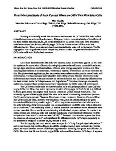
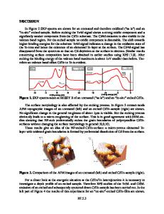
Properties of RF Sputtered ZnTe:N films for Back Contact to CdS/CdTe Solar Cells Jennifer Drayton, A. Gupta, K. Makhratchev, K. J. Price, R. G. Bohn, and A.D. Compaan Department of Physics and Astronomy, The University of Toledo, Toledo, Ohio, 43606 ABSTRACT Most of the low resistance back contacts formed on high efficiency CdS/CdTe solar cells involve copper either in elemental form (such as Cu/Au back contacts) or as dopant in other material (such as Cu-doped ZnTe). But copper is also suspected to be a cause of degradation of devices in long-term stability tests due to its high diffusion coefficient in polycrystalline CdTe. In this paper, we present results on the development of nitrogen-doped ZnTe back contacts for CdS/CdTe solar cells. Reproducible N-doped p-ZnTe films were prepared using reactive RF magnetron sputtering with Ar/N2 gas mixtures. The conductivity of the doped ZnTe films was more than five orders of magnitude higher than that of intrinsic films. We find that annealing in air can further increase the conductivity. Efficiencies near 10% have been achieved with a ZnTe:N/Ni back contact. INTRODUCTION CdTe is a high work-function semiconductor and the p-type material is difficult to contact. Most commonly used contacts to polycrystalline thin-film CdTe utilize copper in some way, either as part of the contact itself or to achieve p+ doping of the CdTe adjacent to the contact. Meyers [1], however, has shown that ZnTe can be used to fabricate high efficiency polycrystalline thin-film solar cells by electrodeposition. Also, Gessert’s group [2] has successfully used ZnTe doped with copper as part of a back contact to CdTe cells. However, Gessert, et al [2] have also shown that there is considerable diffusion of Cu from the ZnTe:Cu into both the CdTe and CdS layers, which occurs during the ~400 oC deposition of the ZnTe. There is concern that this copper may lead to some stability problems in the CdS/CdTe/ZnTe:Cu/Ti devices. Recently atomic nitrogen has been quite successfully used to dope ZnSe and ZnTe during MBE growth.[3] Although electron-cyclotron-resonance plasma sources of atomic nitrogen have proven very successful for doping of epitaxial films,[4] it is challenging to achieve effective doping in a sputtering environment with abundant gas collisions and in polycrystalline thin films with the ever-present grain boundary traps. In this paper we report on the properties of thin films of reactively sputtered ZnTe:N on glass [5] and on the successful use of this ZnTe:N for back contacts to polycrystalline CdTe thin-film cells [6,7] in which no intentional copper has been used in the CdTe or back contact. By using ZnTe:N as a back contact instead of elemental Cu, we hope to fabricate CdS/CdTe solar cells with better stability. In a recent paper, we reported initial results for contacts utilizing a layer of ZnTe:N [8]. Subsequently we have found the characteristics of the films to be very sensitive to contamination from metal sputtering which was being done in the same chamber. We report here on new measur
Data Loading...