Electronic Properties of Chemically Etched CdTe Thin Films: Role of Te for Back-Contact Formation
- PDF / 281,633 Bytes
- 6 Pages / 612 x 792 pts (letter) Page_size
- 72 Downloads / 332 Views
Electronic Properties of Chemically Etched CdTe Thin Films: Role of Te for Back-Contact Formation D. Kraft1, A. Thißen1, M. Campo2, M. Beerbom1, T. Mayer1, A. Klein1 and W. Jaegermann1 1 Department of Materials Science, Darmstadt University of Technology, Petersenstr. 23, D-64287 Darmstadt, Germany 2 ANTEC Technology GmbH, Arnstädter Str. 22, D-99334 Rudisleben, Germany
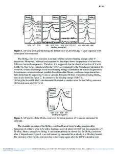
ABSTRACT Improvement of electric back contact formation is one of the major issues of the CdTe thin film solar cell research. Chemical etching of CdTe before metallization is accepted to improve contact formation. It is believed that a CdTe/Te contact is formed by this procedure leading to a Fermi level position in the CdTe close to the valence band maximum for low contact resistance. We have studied the electronic properties of chemically etched CdTe surfaces with photoelectron spectroscopy. Etching of the samples was performed in air (“ex-situ“) as well as in an electrochemical setup directly attached to the UHV system (“in-situ“). The formation of a Te layer is clearly shown by (S)XPS. In contrast to previous studies we could not detect the formation of a p-CdTe surface for different experimental conditions. The detected Fermi level position indicates still band bending and hence a blocking Schottky barrier.
INTRODUCTION The advantage of polycrystalline thin film solar cells like CdTe-based cells compared to conventional devices are a reasonable conversion efficiency of about 10% and above reached by a low cost production process [1-4]. Besides the issues of morphology and lateral inhomogeneities knowledge of the band energy diagrams of solar cells is essential for a fundamental understanding of their function. The commonly used CdTe cell setup is composed of a float-glass substrate with the transparent front contact, usually an ITO layer with a SnO2 diffusion barrier and the converting heterocontact CdS/CdTe [4,5]. A subsequent CdCl2-activation step is necessary for a good cell performance. Finally the backcontact is formed. Main limitation of the conversion efficiency seems to occur due to "non-ohmic" backcontacts. Therefore comparative studies of different preparation procedures and different backcontact materials with high work functions have to be carried out. In previous studies [1-5,7] a p-doped surface layer of CdTe has been quoted. In this report the influence of wet-chemical etching with NP-etch of the CdTe-film before deposition of the backcontact material is investigated. This technique is used in many CdTesolar cells production lines [4] and has been studied in some earlier works[6-10].
EXPERIMENTAL DETAILS The samples used in this study were taken from the CdTe thin film solar cell production line of ANTEC GmbH. The conducting Indium Tin Oxide (ITO) layer and the Tin Dioxide buffer H7.5.1
layer (SnO2) were deposited onto a commercial glass substrate by a sputtering process. Afterwards the heterojunction layers CdS and CdTe were formed using Close Space Sublimation (CSS) [4] followed by a Cadmium Chloride (CdCl2) activation step.
Data Loading...