Pulsed Ion Beam Interface Melting of PtCr and CrTa Alloys on Si Structures
- PDF / 303,657 Bytes
- 6 Pages / 420.48 x 639 pts Page_size
- 81 Downloads / 281 Views
C. J. PALMSTROM AND R. FASTOW Department of Materials Science and Engineering, New York 14853
Cornell University,
Ithaca,
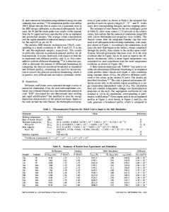
ABSTRACT Composition profiles of thermal and pulsed ion beam annealed PtCr/Si and CrTa/Si have been determined using Rutherford backscattering analysis. Thermal annealing resulted in layered phase separation with Pt-silicide in the PtCr/Si case, and CrSi 2 in the CrTa/Si case, forming at the Si surface. Pulsed ion beam annealing, 2 300-380 keV protons at energy densities "-0.75-1.6 J/cm , produced interface melting with no layered phase separation.
INTRODUCTION For energetic light ions impinging on a material surface, their energy is deposited relatively uniformly in depth up to the ion range ("-3pm for 300 keV H in Si). Hence, unlike laser annealing, where all the energy is primarily deposited at the surface, pulsed ion beam annealing may be considered as a rapid thermal heating of the surface region. This technique, with typi~al %200-400ns pulses of 300-380 keV H ions with energy densities J/cm , has been used successfully to anneal ion implanted Si (1,2) and single metals on Si (2-4). Chen et al. (3,4) observed that by tailoring the energy density of the pulsed ion beam, epitaxial NiSi 2 could be formed on Si. For pulsed ion beam annealing of Si using 200ns proton pulses with energy 2 density "-1.5 J/cm the surface remains molten for a duration of "'ivs (5). 2 This time regime requires diffusion coefficients > 10-5 cm /sec in the metal-Si reactions. Baglin et al. (2) suggested that a melt starts at the metal-Si interface and that the amount of melt increases with increasing energy density. Studies have been made on metal alloy films on Si in the hope of limiting the Si consumption during silicide formation and hence producing a shallow silicide contact (6). The principle behind this idea is that by using an alloy of two metals, one which forms a silicide at relatively low temperature (Tk), and another which forms a silicide at high temperature (Tb), the consumption of Si can be limited during contact silicide formation. Thus, when the metal alloy/Si structure is heated above T., but below Tb, the low temperature metal silicide starts to form at the Si-alloy interface, the growth of the silicide being limited by the amount of this metal present. The thin silicide layer so formed is believed to determine the electrical behavior of the contact. Most studies have been on alloys comprising a near noble and refractory metal (e.g. PtCr, PtW, PtV, PdCr, PdW, PdV or NiCr (6-11). In general, the near noble metal silicide forms at the Si surface with a layer rich in the refractory metal silicide forming on top (7). Layered phase separation is also observed for IrV alloys (12) and is suggested for GdPt alloys on Si (13). In the particular case of TiW alloys, a ternary phase, Tio.3 WO.7 Si, has been observed to form (14). The present study has been made to see whether layered phase separation can be achieved by melting of the alloy/Si interface using pulsed ion beam annealing. Here we compare the comp
Data Loading...