Mo-Si Interface Formation by Ion Beam Sputter Deposition
- PDF / 3,596,152 Bytes
- 6 Pages / 612 x 792 pts (letter) Page_size
- 112 Downloads / 364 Views
W17.12.1
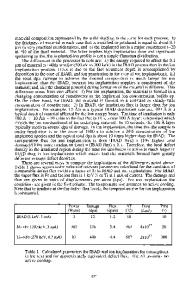
Mo-Si Interface Formation by Ion Beam Sputter Deposition A. Köhler, J.W. Gerlach, T. Höche, T. Chassé, H. Neumann, W. Frank, G. Wagner, and B. Rauschenbach Institute for Surface Modification, Permoserstr. 15, D-04318 Leipzig ABSTRACT Molybdenum-silicon (Mo-Si) multilayers for EUV lithography were prepared by ion beam sputter deposition at room temperature. The multilayer structure was determined by X-raydiffraction and transmission electron microscopy. Textured molybdenum layers with preferential (110) orientation normal to the surface are observed. At the interfaces of all Mo-Si and Si-Mo pairs additional intermixing resulting in molybdenum silicide layers were noticed. These layers have a thickness of about 0.7 and 1.5 nm each, respectively. Due to this intermixing, the nominal thickness of the Mo and Si layers is reduced. The optical index contrast at the interface is also expected to decrease. This is in accordance with the obtained EUV reflectivity results of 64-65% at 13.4 nm which remains below the theoretical value of 74%. The formation of the silicide interface layers is discussed and an optimized deposition process focused on narrowing these transition layers is suggested. INTRODUCTION Mo-Si multilayer stacks are to be applied as optical elements (mirrors, mask blanks) for extreme ultraviolet light lithography (EUVL). EUVL is one of the leading candidates for next generation lithography (NGL) which is expected to enable structural widths of down to 30 nm. The multilayers have to yield a high reflectivity at a wavelength of 13.4 nm. To optimize the optical properties a detailed investigation of the multilayer microstructure is required. One important characteristic of the Mo-Si multilayer deposition is the formation of transition layers at the Mo-Si interfaces. In the present study, Mo-Si multilayers prepared by ion beam sputter deposition are investigated by high resolution transmission electron microscopy. The microstructure characterization is completed by X-ray and EUV reflectivity measurements. EXPERIMENTAL DETAILS The Mo-Si multilayer stacks discussed in this study were prepared by ion beam sputter deposition. The experiments were performed in a commercial dual ion beam deposition (DIBD) system with a base pressure below 10-8 mbar. The DIBD system was equipped with special ECR ion beam sources, which were developed at the Institute for Surface Modification, Leipzig. The individual layers were deposited by xenon ion beam sputtering of pure silicon and molybdenum sputter targets, respectively. The ion energy was in the range of 400 to 1000 eV, while the ion beam current was between 30 and 60 mA. The xenon partial pressure was 3 x 10⁻⁵ mbar during the deposition process. The multilayers were deposited at room temperature onto Si(100) wafers
W17.12.2
with a diameter of 6”. Nominal thicknesses of the molybdenum and silicon single layers were estimated from the deposition rates. The multilayer stacks consist of a silicon buffer layer followed by 50 Mo-Si double layers. The microstructure of the
Data Loading...