A Leed Study of Bismuth Overlayer Formation on InSb(110)
- PDF / 769,072 Bytes
- 6 Pages / 420.48 x 639 pts Page_size
- 117 Downloads / 312 Views
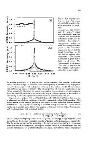
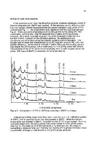
A LEED STUDY OF BISMUTH OVERLAYER FORMATION ON InSb(110) T. Guo, K. J. Wan and W. K. Ford Advanced Materials Center and the Department of Physics Montana State University, Bozeman, Montana 59717 ABSTRACT LEED and Auger electron spectroscopy have been used to studied the interface formation of bismuth on InSb(110). For the first time, well defined superstructures were observed at room temperature on metal/semimetal-III-V semiconductors. A (Wx2)phase, at 0.5 ML bismuth coverage, and a (Wx3)phase, at 0.4 ML bismuth coverage, appear with different thermal heat cycling. The dynamical origin of these phases is thought to be a repulsive interaction between overlayer chains due to the detailed geometry of the overlayer chain structure and to the overlayer induced strain field within the substrate. INTRODUCTION Renewed attention has been given to the interface systems of column-V elements on III-V semiconductor (110) surfaces following the recent discovery of the epitaxial growth of bismuth on the GaAs(110) surface.[1] Although (110) surfaces are convenient to prepare experimentally and to study theoretically, very few elements are known to form ordered overlayers on them. The scarcity of examples of epitaxy reduces the efficacy of the use of the (110) substrate surface to study the microscopic properties of overlayer formation and epitaxial growth, and serves to underscore the importance of detailed bismuth and antimony adatom studies because overlayers of these atoms are epitaxial on several III-V (110) surfaces.[2-4] With the advantages provided by the bismuth and antimony prototype systems studies may proceed that determine more fully the ordering properties, atomic geometries, and chemical bonding in the overlayer. The atomic and electronic structure of antimony on the GaAs(110) and InP(110) surfaces have been studied extensively in the past.[1,31 Antimony forms an ordered p(lxl) - 1ML overlayer that undoes the substrate reconstruction, leaving the surface in a bulk-terminated geometry with zig-zag chains of antimony atoms running along the [110]
direction in the positions normally occupied by gallium and arsenic atoms in the bulk. A clean surface which has not been allowed to relax would have dangling bonds on each of the anion and cation tetrahedral surface sites. This configuration is energetically unstable and a sizable reconstruction occurs for all III-V and I1-VI (110) semiconductor surfaces.[5] In the formation of the antimony overlayer geometry, the dangling bonds are bonded to the overlayer adatom chain in such a way so as to stabilize the truncated bulk geometry.[1,3] A recent dynamical LEED intensity analysis of the Bi/GaAs(110) system shows that bismuth forms a similar zig-zag chain structure but that the chains are punctuated by vacancies every six unit cells giving rise to a "(6xl)" surface geometry.[4,6] The vacancies occur to relieve the strain in the interface that arises due to the size mismatch between the bismuth adatoms and the substrate unit cell size. The ordering of the chain vacancies is the s
Data Loading...


