A simulation study for defects in sub-15 nm line-space using directed self-assembly
- PDF / 1,034,468 Bytes
- 6 Pages / 612 x 792 pts (letter) Page_size
- 109 Downloads / 282 Views
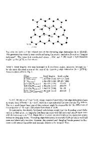
A simulation study for defects in sub-15 nm line-space using directed self-assembly Hideki Kanai, Katsuyoshi Kodera, Yuriko Seino, Hironobu Sato, Yusuke Kasahara, Katsutoshi Kobayashi, Ken Miyagi, Shinya Minegishi, Naoko Kihara, Yoshiaki Kawamonzen, Tomoharu Fujiwara, Noriyuki Hirayanagi, Toshikatsu Tobana and Tsukasa Azuma EUVL Infrastructure Development Center, Inc. (EIDEC), 16-1 Onogawa, Tsukuba, Ibaraki, 305-8569, Japan ABSTRACT A specific type of buried defect in lamellar phase diblock copolymer was studied by experiments and simulations using self-consistent field theory (SCFT). The defects had 3dimensional structures and created hexagonally arranged holes. They existed not only on the substrate with the guide structures but in fingerprints. The simulation results suggested that one of the causes of the defects is mismatch of the surface affinity of the neutral layer. INTRODUCTION Recently, directed self-assembly (DSA) with lamellar phase block copolymer has progressed greatly with regard to its applicability in the manufacturing of semiconductor devices, but the topological defects such as dislocation and disclination remain a major concern. In addition, buried defects [1-3] may appear if the materials and/or the process steps are not optimized for chemo- or grapho-epitaxy flow, and then they will cause poor etch selectivity and degradation of line edge roughness (LER) in pattern transfers into underlayers. Hexagonally perforated lamellae (HPL), one of the typical types of the buried defects, has been investigated with experiments [4] and simulations [5, 6]. HPL is recognized as a metastable state and can be seen with diblock and triblock copolymers. In this study, we discuss defect analysis, in which specific type of buried defect is included. The buried defects arise and are clearly evident on shallowly etched SOG after dry development of PS-b-PMMA diblock copolymers. The analysis is based on self-consistent field theory (SCFT) simulation for the bottom surface affinity with analysis of free energy difference among several phase configurations. EXPERIMENTAL DETAILS PS-b-PMMA diblock copolymers with 1/2∙L0 = 15 nm (L0 is pitch of the copolymers) and OH-terminated PS-r-PMMA as the neutral layer were used. The substrate consisted of spinon-glass (SOG) and spin-on-carbon (SOC) stacked on bare-Si. The EIDEC process flow described in ref. 7 for making 15 nm half-pitch lines and spaces on 90 nm pitch guide structures is as follows. Firstly, photoresist is coated on SOG/SOC stacked wafer and exposed by a novel ArF immersion scanner. The photoresist and the SOG are etched in order to reduce the width to 1/2∙L0. The trimmed photoresist and the SOG work as chemical guides and affinity to PMMA segment of the PS-b-PMMA is induced. They also work as physical guides of grapho-epitaxy. Then, the neutral layer is spin-coated and grafted only on the SOG surface and PS-b-PMMA is coated and thermally annealed to induce microphase separation. Finally, the PMMA is removed by RIE and 15 nm PS lines are formed. In this flow, no sp
Data Loading...