A Study of the Photovoltaic Effect of a Semiconductor Grain Boundary by a Scanning Laser Beam
- PDF / 310,690 Bytes
- 6 Pages / 420.48 x 639 pts Page_size
- 21 Downloads / 366 Views
found resulting from dislocations
or impurity segregations. (5,61 The charge at interface states produces a potential barrier which impedes majority carrier current flow, thus reducing mobility and increasing resistivity. These interface states also behave as very effective recombination centers lowering the overall minority carrier lifetime and diffusion length.i
4
'
7 8 1
'
Among the methods used to
measure the grain boundary parameters,( 9 ' 1 0 ' 1 1 ' 1 2 ' 1 3 1 the application of a laser beam has many advantages. Sample preparation is simple, and the carrier generation and profile are well characterized. Also, a highly focused laser beam allows us to examine individual grain boundary in a sample containing multiple grains. In this paper, we will present a model for the photovoltaic effect of a grain boundary caused by a scanning laser beam, which can be used to measure diffusion length within a grain and recombination velocity at a grain boundary. THEORY Let us consider a p-type silicon bicrystal sample with a grain boundary across the whole width. The holes trapped at the interface states of the grain boundary give rise to a potential barrier which impedes carrier transport. The grain boundary potential barrier may be represented by back-to-back Schottky diodes as shown in Fig. la. When excess carriers are produced in one side of the grain boundary by a laser beam (Fig. lb), the potential barrier on that side of the grain boundary is reduced giving rise to the photovoltaic effect (Fig. 2).
Mat. Res. Soc. Symp. Proc. Vol. 54. ' 1986 Materials Research Society
658
_
R-0
0)
_
_
_
_
_
_
_
_
_
_
_
_
_
E,O "
0
Ec
S I
,.I
I
•
•
.2
Ep
b)
-6 -5 -4 -3 -2 -1 G0 1 2 3 4 5 6 DISTANCEOF THE LASER BEAMFROM THE GRAINBOUNDARY (mils)
7
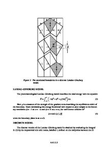
Fig. 2. An example of photovoltaic effect of a grain boundary. Fig. 1. (a)Electron energy diagram near a grain boundary in the The dark. (b)The geometry of the sample under illumination. shaded area represents a small section of the grain boundary where VD D is calculated. Assuming a point source of excess carriers generated at (x 0 ,0,0), the continuity equation for the steady state excess minority carrier concentration is DAn(x,y,z)/Dt = DnV2[An(x,y,z)] + (l-R)nG6(x-x Dn is
- An(x,y,z)/Tn 0
)6y6z
minority carrier diffusion constant,
(1) T
is
minority carrier
lifetime, i is internal quantum efficiency, R is reflectivity of This equation may be the surface and. G is incident photon rate. solved by regarding the grain boundary and the depletion layers The boundary as a single plane with a recombination velocity s. conditions for this problem are deduced from the following assumptions: assumed to be
1.
The recombination at the free surface is negligible.
2.
The excess minority carriers at depletion layer edges on both sides of the grain boundary are the same because the width of the depletion layers is much narrower than diffusion length.
3.
The recombination in a depletion layer is negligible because a depletion layer is much narrower than di
Data Loading...


